High precision CCD automatic positioning, automatic focusing. Fast and accurate positioning, save time and no worries. Friendly interface,Simple operation, easy to use, free application; Small size, Save more space; rigorous security design. Reduce

Compared with conventional tools, laser processing offers a compelling series of advantages. The laser process is completely software-controlled. Varying materials or cutting contours are easily taken into account through adaptation of the proce
Electronics Forum | Sun Sep 22 02:32:33 EDT 2013 | alexeis
Hi, If your PCB is large, you waste a time. Any picture, you takes, will be with corner distortion. I suggest you to: 1. use AOI (manually or automatically) 2. try simulation of your PCB production before real SMT production process 3. use human FAI
Electronics Forum | Mon Sep 13 04:11:27 EDT 1999 | Earl Moon
| | hello | | | | having a problem with one customers bare boards not matching my stencil apertures. i design stencils based on gerber data and reduce up to 15% on some pads. do some board houses reduce pads after receiving gerber data???why would
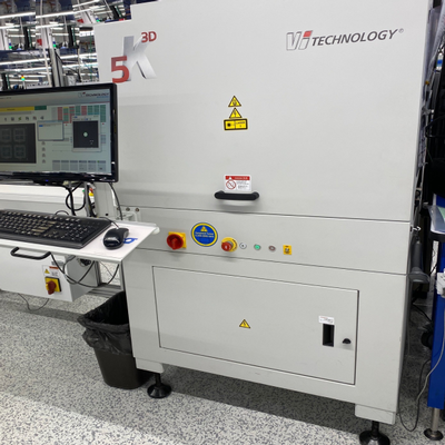
Used SMT Equipment | AOI / Automated Optical Inspection
Make: Vi Technology Model: 5K 3D AOI Vintage: 2017 Details: Precision XY Gantry High-Speed Linear Motors with Closed-Loop, High-Resolution Linear Encoders Automatic Conveyor Width Adjust Large Board! Max Bo
Used SMT Equipment | Screen Printers
Description Make: Speedprint Model: SP710 AVI Year: 2014 Type: Screen Printer
Industry News | 2007-11-04 19:25:08.0
Aesch/Switzerland � Essemtec AG, a leading manufacturer of surface mount technology production equipment, announces that it will highlight SP900 inline printer in booths A5-277 and A5-278 at the upcoming Productronica 2007 exhibition and conference scheduled to take place November 13-16, 2007 at the New Munich Trade Fair Center in Munich, Germany.
Industry News | 2010-03-27 16:25:11.0
MARTIN, a FINETECH company, will demonstrate the new Expert 10.6XL Rework System in booth #638 at the upcoming IPC/APEX exhibition, scheduled for April 6-8, 2010 at the Mandalay Bay Convention Center in Las Vegas, NV.

Parts & Supplies | Assembly Accessories
After receiving the input signal of home sensor of motor related to head, it is transmitted to can master BOARD.CONVEYOR Control board receive controller The sensor input with ANC and the input of the switch on the operation panel are transmitted t
Technical Library | 2021-06-21 19:34:02.0
In this era of electronics miniaturization, high yield and low-cost integrated circuit (IC) substrates play a crucial role by providing a reliable method of high density interconnection of chip to board. In order to maximize substrate real-estate, the distance between Cu traces also known as line and space (L/S) should be minimized. Typical PCB technology consists of L/S larger than 40 µ whereas more advanced wafer level technology currently sits at or around 2 µm L/S. In the past decade, the chip size has decreased significantly along with the L/S on the substrate. The decreasing chip scales and smaller L/S distances has created unique challenges for both printed circuit board (PCB) industry and the semiconductor industry. Fan-out panel-level packaging (FOPLP) is a new manufacturing technology that seeks to bring the PCB world and IC/semiconductor world even closer. While FOPLP is still an emerging technology, the amount of high-volume production in this market space provide a financial incentive to develop innovative solutions in order to enable its ramp up. The most important performance aspect of the fine line plating in this market space is plating uniformity or planarity. Plating uniformity, trace/via top planarity, which measures how flat the top of the traces and vias are a few major features. This is especially important in multilayer processing, as nonuniformity on a lower layer can be transferred to successive layers, disrupting the device design with catastrophic consequences such as short circuits. Additionally, a non-planar surface could also result in signal transmission loss by distortion of the connecting points, like vias and traces. Therefore, plating solutions that provide a uniform, planar profile without any special post treatment are quite desirable.
Technical Library | 2020-07-08 20:05:59.0
There is a compelling need for functional testing of high-speed input/output signals on circuit boards ranging from 1 gigabit per second (Gbps) to several hundred Gbps. While manufacturing tests such as Automatic Optical Inspection (AOI) and In-Circuit Test (ICT) are useful in identifying catastrophic defects, most high-speed signals require more scrutiny for failure modes that arise due to high-speed conditions, such as jitter. Functional ATE is seldom fast enough to measure high-speed signals and interpret results automatically. Additionally, to measure these adverse effects it is necessary to have the tester connections very close to the unit under test (UUT) as lead wires connecting the instruments can distort the signal. The solution we describe here involves the use of a field programmable gate array (FPGA) to implement the test instrument called a synthetic instrument (SI). SIs can be designed using VHDL or Verilog descriptions and "synthesized" into an FPGA. A variety of general-purpose instruments, such as signal generators, voltmeters, waveform analyzers can thus be synthesized, but the FPGA approach need not be limited to instruments with traditional instrument equivalents. Rather, more complex and peculiar test functions that pertain to high-speed I/O applications, such as bit error rate tests, SerDes tests, even USB 3.0 (running at 5 Gbps) protocol tests can be programmed and synthesized within an FPGA. By using specific-purpose test mechanisms for high-speed I/O the test engineer can reduce test development time. The synthetic instruments as well as the tests themselves can find applications in several UUTs. In some cases, the same test can be reused without any alteration. For example, a USB 3.0 bus is ubiquitous, and a test aimed at fault detection and diagnoses can be used as part of the test of any UUT that uses this bus. Additionally, parts of the test set may be reused for testing another high-speed I/O. It is reasonable to utilize some of the test routines used in a USB 3.0 test, in the development of a USB 3.1 (running at 10 Gbps), even if the latter has substantial differences in protocol. Many of the SI developed for one protocol can be reused as is, while other SIs may need to undergo modifications before reuse. The modifications will likely take less time and effort than starting from scratch. This paper illustrates an example of high-speed I/O testing, generalizes failure modes that are likely to occur in high-speed I/O, and offers a strategy for testing them with SIs within FPGAs. This strategy offers several advantages besides reusability, including tester proximity to the UUT, test modularization, standardization approaching an ATE-agnostic test development process, overcoming physical limitations of general-purpose test instruments, and utilization of specific-purpose test instruments. Additionally, test instrument obsolescence can be overcome by upgrading to ever-faster and larger FPGAs without losing any previously developed design effort. With SIs and tests scalable and upward compatible, the test engineer need not start test development for high-speed I/O from scratch, which will substantially reduce time and effort.
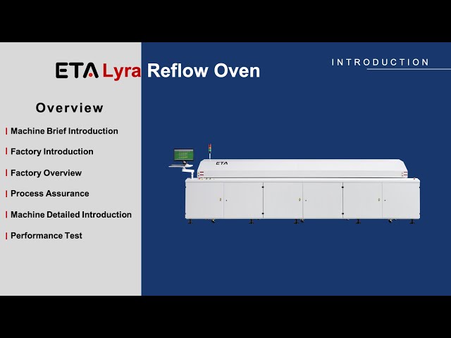
S8, S10, S12 - 8, 10 or 12 top/bottom cooling zones. Heating System: Up to twelve groups of top and bottom forced hot air convection heating zones. Patented heating plates in each zone uniformly transfer heat to the PCBs using forced hot air con
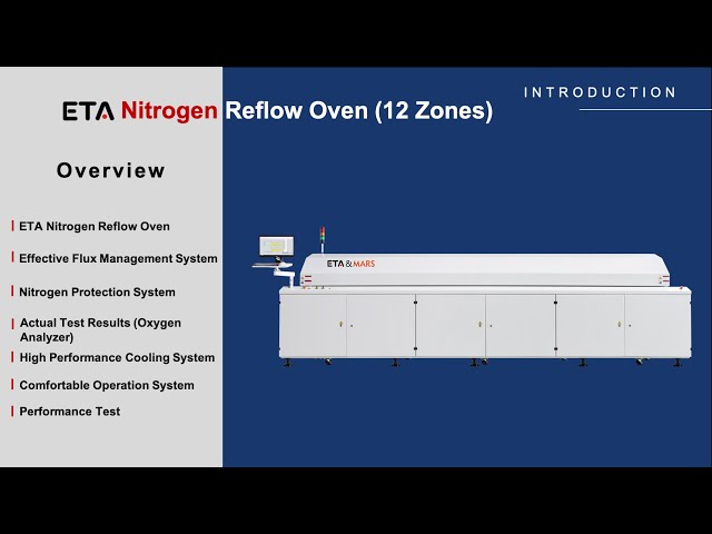
E8, E10, E12 - 8, 10 or 12 top/bottom cooling zones. Heating System: Up to twelve groups of top and bottom forced hot air convection heating zones. Patented heating plates in each zone uniformly transfer heat to the PCBs using forced hot air con
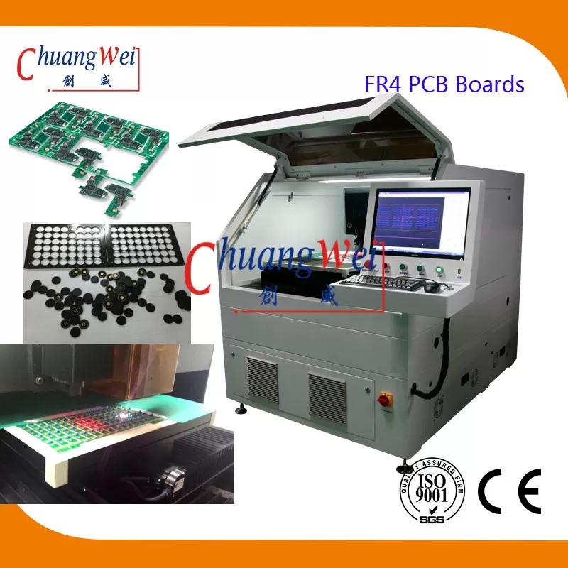
| https://www.smtfactory.com/High-Speed-SMT-AOI-Machine-in-PCB-Board-Off-Line-Model-I-C-T-V8-pd48670624.html
High Speed SMT AOI Machine in PCB Board Off-Line Model I.C.T-V8 from China manufacturer - I.C.T English Français Pусский Español Português Deutsch Italiano 日本語 한국어 Tiếng Việt Türk dili Home About Us Company Profile
Imagineering, Inc. | https://www.pcbnet.com/blog/controlling-signal-integrity-in-high-speed-pcb-design/
. Ideally, a printed circuit board will have no signal distortion, can handle electromagnetic interference from nearby devices, and does not generate significant interference of its own


winsouce.jpg)