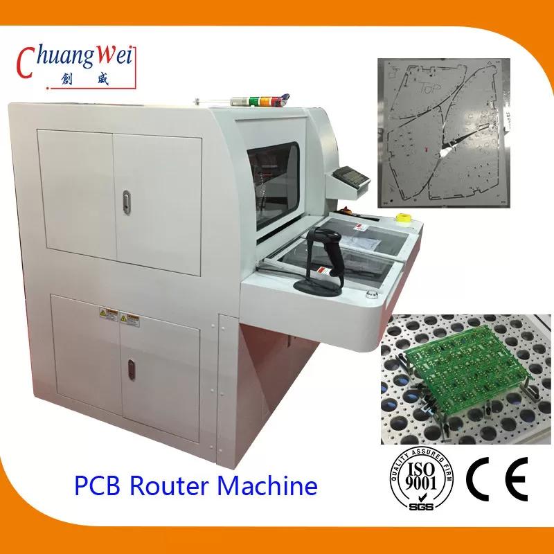
Double Station PCB Router Machine with Auto Routing Bit Checker PCB Router Machine Description 2-way Sliding Exchanger This work exchanger provides a simultaneously in-and-out working space to limit the idle time, which in turn reaches the utmost o
Features : 1. Two-slide PCB Separator 2. Low stress 3. Sharp cutting edge 4. Manul loading /unloading 5. High speed cutting by 4 axes control 6. Easy teaching with image processing Description: 2-way Sliding Exchanger This work exchanger pro
Electronics Forum | Sun May 24 06:02:33 EDT 1998 | Earl Moon
| Hello, | I am looking for suggestions for cleaning pcb's after the routing (fabrication) process. Keep in mind that these pcb do not have components intalled on them yet. | We have considered pre-drilling the routing plunge points, but cost and ca
Electronics Forum | Thu Mar 20 17:39:41 EDT 2008 | boardhouse
FSW, Another suggestions is if you have rail on your product and you are concerned about stress fracturing certain components you could add a routed slot to add relief in that area. So when you snap the rail off their would be no stress in that area
Used SMT Equipment | General Purpose Equipment
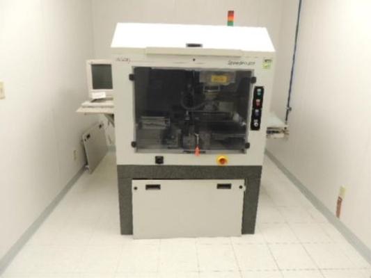
IPTE High Speed Router Equipment Description IPTE Model Number: NTM 4133 Serial Number: 6000 741 Year: 2002 Type: Fully Automatic HIgh Speed PC Board Windows O/S Routing Area: 410 x 330 mm Sawing Area: 360 x 330 mm
Industry News | 2003-03-11 08:45:00.0
CAMtastic DXP is the latest version of Altium's complete CAM verification and editing system that bridges the gap between PCB design and manufacturing and facilitates communication between board designers, fabrication engineers, and their clients.
Industry News | 2022-02-10 17:06:48.0
Rafal Przeslawski, Xilinx takes top prize
Technical Library | 2021-09-02 08:17:07.0
We are a professional manufacturer of PCB depaneling machines, which is workable for all boards, including flex and regid boards, v-scored boards and routed boards. Laser pcb depaneling is non-contact way without mechanical stress,this solution is good for modern precision PCB depaneling. It has below advantages: 1. No dust The production environment of the circuit board industry is carried out in the dust-free workshop. The traditional pcb depaneling equipment, such as blade moving type machine, will inevitably produce residues and micro powder, which will pollute the 10000 and 1000 class dust-free workshops and affect the conductivity of products. The UV laser PCB cutting machine is a vaporization processing process, which will not produce dust and is conducive to the conductivity of the product. 2. High cutting precision The processing gap of high-precision traditional processing equipment can not reach the gap width of less than 100 microns, which will cause certain damage to the lines on the edge or PCBA circuit board containing components. The focus spot of the laser cutting machine is small, and the ultraviolet cold processing mode has little thermal impact on the edge of the circuit board. The cutting position accuracy is less than 50 microns, and the cutting size accuracy is less than 30 microns, which will not affect the edge of the circuit board, and the precision is high. 3. No stress Traditional processing methods generally have V-grooves, which will cause certain damage to the board in the manufacturing process. The UV laser PCB cutting machine can directly cut the bare board without making V-grooves. In addition, the traditional processing methods directly use tools to act on the circuit board, especially the stamping method has a great impact on the circuit board, which is easy to cause board deformation. The laser cutting machine is a non-contact processing mode, which acts on the surface of the material through the high-energy beam, which will not cause the influence of stress and the deformation and damage of the circuit board. 4. For special-shaped cutting, it is easy to automate The UV laser PCB cutting machine can cut for any shape without replacing any props and fixtures, and without steel mesh. The same equipment can meet special-shaped and straight-line cutting, which is easy to realize assembly line automatic production and high flexibility. It is easy to improve production efficiency and save production process and production cycle. In particular, it can quickly and efficiently meet the needs of rapid proofing, directly import the drawing, and then locate the cutting. 5. High compatibility The UV laser PCB cutting machine can process the materials around the circuit board, such as PCB, FPC, covering film, pet, reinforcing board, IC, ultra-thin metal cutting, etc. it has strong practicability, is compatible with the processing of a variety of materials, is easy to operate, can be imported into the drawing, does not need to adjust any mechanical parts, and is easy to operate and maintain. 6. Good cutting edge effect The cutting edge is smooth and neat without burr. It can be processed and formed directly according to the size of the drawing, which is conducive to improving the yield of the product. It can be directly installed into the subsequent process without further processing. For more details about UV laser depaneling, please feel free to contact us. www.pcbdepanelingrouter.com
Guillotine type V-cut PCB Cutting Machine Product Description 1. For internal strength generates during separation, Minimize it to value under 180uE ,to avoid solder crack or component damage 2. Able to separate edge of V-slot, minimum distance to

Singulate Straight Tab Routed Panels Store cut tabs inside tool for discarding at operator convenience Available with 3 blade types and choice of support dies Clean cut - requires no rework for deburring PCB edges Easy blade change in under 5 m
Training Courses | | | PCB Rework and Hand Soldering Courses
The PCB rework and hand soldering courses courses cover techniques of rework and repair of PCBs, BGAs and other electronics assemblies, and teach fundamentals of soldering of electronics assemblies.
Training Courses | ON DEMAND | | IPC-600 Trainer (CIT)
The Certified IPC-600 Trainer (CIT) courses recognize individuals as qualified trainers in the area of quality assurance of bare printed circuit boards and prepare them to deliver Certified IPC-600 (CIS) training.
Career Center | San Jose, CA, California USA | Engineering,Production,Research and Development
Senior PCB Designer: Want to be part of an exciting pre-IPO enterprise B2B company working on the cutting edge of internet-of-things, artificial intelligence & agents, blockchain, and manufacturing technology? This well-funded venture-backed co
Career Center | Erode, Tamilnadu India | Engineering
Professional Summary 3+ years of experience in the PCB CAM engineering Exposure to FRONTLINE GENESIS 2000 Having exposure in UCAM Exposure to Create, Array & Panelize it for manufacturability Experienced in Creating impedance cou
SMT Express, Issue No. 2 - from SMTnet.com Volume 1, Issue No. 2 Wednesday, July 14, 1999 Featured Article Return to Previous Page PRINTED CIRCUIT BOARD FABRICATION BASICS AN OUTLINE Earl Moon Proof Of Design (POD) PURPOSE AND SCOPE
, Nick Munson, Steve Ring, Evan Briscoe.; Foresite In
1st Place Machinery Inc. | http://www.firstplacemachinery.com/firstplace_ipte_router.html
Routing Area: 410 x 330 mm Sawing Area: 360 x 330 mm PCB: 410 x 330 mm Vision System for teaching and/or fiducial recognition Adjustable Edge Belt with Flat Belt Conveyor for outfeed Vacuum Cleaner Includes Manuals and Documentation 208/400V - 50/60 HZ - 3
44053 | http://fknsystek.com/8DSR100.pdf
FKN Systek


