Industry Directory | Manufacturer
Industrial Sensor Vision International specializes in advanced camera technology of high resolution fast speed cameras for automation, AOI, 2-D/3-D, SPI inspection and wafer inspection.
Industry Directory | Other / Consultant / Service Provider / Manufacturer
ScanCAD is an industry leader in inspection, measurement, process control and reverse engineering. Our solutions support OEM's, manufacturers, stencil fabricators, repair depots, and others in optimizing quality and yield.
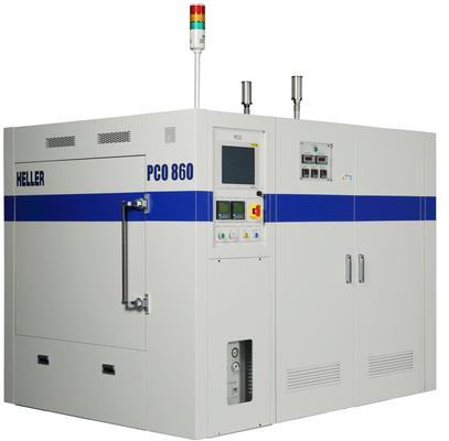
New Equipment | Curing Equipment
A Pressure Cure Oven (PCO), or Autoclave, is used to minimize voiding and increase adhesion strength for bonding processes typically used in die attach and underfill applications. PCO pressurizes air into a rigid vessel and heats & cools with
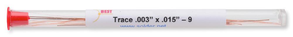
New Equipment | Rework & Repair Equipment
BEST PCB circuit traces are designed to help you repair, replace and modify circuit traces on PCBs. These materials allow you to meet original PCB quality standards as the board side is microetched for improved bonding area and bond strength. The re

Used SMT Equipment | Soldering - Selective
Hot Bar Soldering Flex Circuit to PCB Ribbon Cable to PCB Coaxial Cables Fine Pitch SM Devices Edge Connectors to PCB Thermocompression Bonding Tab to PCB, HSC to LCD or tab More information pjbril@smtunion.com m.madera@smtunion.com W
Used SMT Equipment | Labeling Systems
CBP / TP 5Kg Cold Bump Pull/ Tweezers Pull Cartridge along with JAW Nordson Dage 4000 Bond Tester DAGE 4000 CBP/TP 5KG Qty:2 Condition : Excellent working condition with many Modules all form Europe user Email:13560819457@139.com
Industry News | 2010-12-07 14:53:07.0
GPD Global announces that its Positive Cavity Displacement (PCD) technology is proven with silver-filled electrically and thermally conductive adhesives.
Industry News | 2003-06-10 08:39:25.0
New from Unitek Eapro is a series of desktop systems for hot bar bonding applications.
Technical Library | 2023-08-16 18:48:50.0
One of our aerospace customers was looking to automate a few manual operations and asked for suggestions. This customer specializes in assemblies for inflight connectivity for commercial airlines and low orbit satellites. The dispensing process included the application of bonding to the sides of large and small components (4-axis) and the ability to cope with the changing viscosity during processing. The material used was EC-2216 B/A Two Part Epoxy and the largest board size was 12"x10"
Technical Library | 2020-08-27 01:22:45.0
Initially adopted internal specifications for acceptance of printed circuit boards (PCBs) used for wire bonding was that there were no nodules or scratches allowed on the wirebond pads when inspected under 20X magnification. The nodules and scratches were not defined by measurable dimensions and were considered to be unacceptable if there was any sign of a visual blemish on wire-bondable features. Analysis of the yield at a PCB manufacturer monitored monthly for over two years indicated that the target yield could not be achieved, and the main reasons for yield loss were due to nodules and scratches on the wirebonding pads. The PCB manufacturer attempted to eliminate nodules and scratches. First, a light-scrubbing step was added after electroless copper plating to remove any co-deposited fine particles that acted as a seed for nodules at the time of copper plating. Then, the electrolytic copper plating tank was emptied, fully cleaned, and filtered to eliminate the possibility of co-deposited particles in the electroplating process. Both actions greatly reduced the density of the nodules but did not fully eliminate them. Even though there was only one nodule on any wire-bonding pad, the board was still considered a reject. To reduce scratches on wirebonding pads, the PCB manufacturer utilized foam trays after routing the boards so that they did not make direct contact with other boards. This action significantly reduced the scratches on wire-bonding pads, even though some isolated scratches still appeared from time to time, which caused the boards to be rejected. Even with these significant improvements, the target yield remained unachievable. Another approach was then taken to consider if wire bonding could be successfully performed over nodules and scratches and if there was a dimensional threshold where wire bonding could be successful. A gold ball bonding process called either stand-off-stitch bonding (SSB) or ball-stitch-on-ball bonding (BSOB) was used to determine the effects of nodules and scratches on wire bonds. The dimension of nodules, including height, and the size of scratches, including width, were measured before wire bonding. Wire bonding was then performed directly on various sizes of nodules and scratches on the bonding pad, and the evaluation of wire bonds was conducted using wire pull tests before and after reliability testing. Based on the results of the wire-bonding evaluation, the internal specification for nodules and scratches for wirebondable PCBs was modified to allow nodules and scratches with a certain height and a width limitation compared to initially adopted internal specifications of no nodules and no scratches. Such an approach resulted in improved yield at the PCB manufacturer.
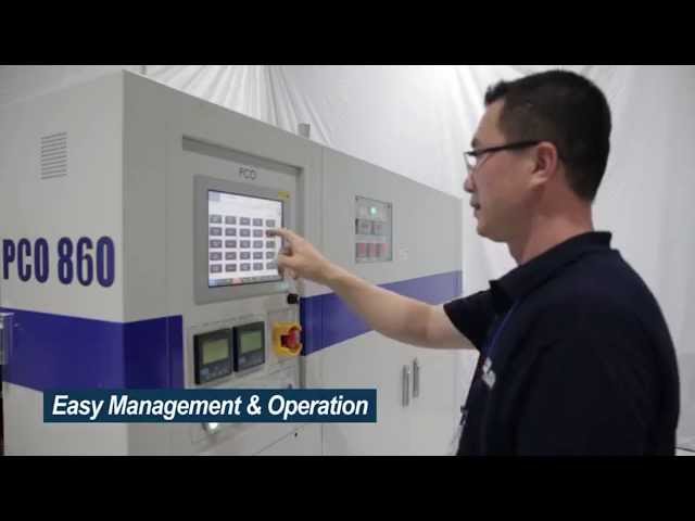
General curing, die attach curing, underfill curing, film & tape bonding, wafer laminating.

PCB pad circuit repair using epoxy. Using multiple angles including overhead and from both right and left angles the BEST instructor staff demonstrates plainly how to repair a PCB pad using the epoxy method. This method is per IPC 7721 4.4.1. http://
Training Courses | | | Other Courses
Other courses related to electronics manufacturing and assembly
Training Courses | | | ESD Control Training Courses
Browse training and certification programs for electrostatic discharge (ESD) control in electronics assembly.
Events Calendar | Tue Aug 20 18:30:00 UTC 2024 - Tue Aug 20 18:30:00 UTC 2024 | Kaohsiung City, Taiwan
Taiwan Alliance LTS Workshop
Events Calendar | Mon Jun 27 18:30:00 UTC 2022 - Wed Jun 29 18:30:00 UTC 2022 | Novi, Michigan USA
Adhesives & Bonding Expo
Career Center | Philadelphia, New Jersey USA | Sales/Marketing
LOCATION BASE SALARY USA - NJ - Central USA - NJ - Southern USA - PA - Philadelphia $67000 - 73000 Another $50K to $70K in commissions based on plan COMPANY BRIEF My client is a leading supplier of automated broadband communications assembly e
Career Center | Boise, Idaho USA | Engineering
In need of a contract engineer ASAP!! This person will help with the fabrication of implantable medical devices. Incumbent must have electronic packaging and uBGA experience. The qualifications are below. This position will be from 3-9 months and nee
Career Center | Littleton, CO USA | Production
Possess 18 years relevant work experience in manual/Auto bonding on Micro-Electronic & RF to support new product development in R&D Lab in defense & commercial sectors. Have an advanced soldering skill in both Through-Hole/SMT, and J-STD-001 cert
Career Center | Folsom, California USA | Engineering,Production
A skilled electronics industry worker with experience in solder assembly, rework, and wire-bond. Accustomed to working in both production and engineering envrionments on commercial and military products.
SMT Express, Volume 2, Issue No. 9 - from SMTnet.com Volume 2, Issue No. 9 Thursday, September 14, 2000 Featured Article Return to Front Page Book Review Reviewed by Dave Fish (davef ), Pandion Electronics, Inc Title: Wire Bonding
| https://www.eptac.com/faqs/ask-helena-leo/ask/gold-wire-bond-failing-pull-test
Gold Wire Bond Failing Pull Test - EPTAC - Train. Work Smarter. Succeed Looking for solder training standards, manuals, kits, and more
KingFei SMT Tech | http://www.smtspare-parts.com/sale-8530771-strong-adhesive-bond-smt-cover-tape-extender-8mm-smt-joint-tape-black-esd.html
Strong Adhesive Bond SMT Cover Tape Extender 8mm SMT Joint Tape Black ESD Leave a Message We will call you back soon! Your message must be between 20-3,000 characters
1.jpg)


