
Industry Directory | Consultant / Service Provider / Manufacturer / Other
ScanCAD is an industry leader in inspection, measurement, process control and reverse engineering. Our solutions support OEM's, manufacturers, stencil fabricators, repair depots, and others in optimizing quality and yield.
Industry Directory | Manufacturer
An innovative thermal management company that is dedicated to address the thermal challenges that the electronics industry is facing.

We are well versed in the following thermal application materials: Sil-Pad thermally conductive insulators Gap-Pad thermally conductive gap filling material Q-Pad thermal grease replacement film Bond-Ply thermally conductive adh

The PCB Footprint Expert is a powerful CAD library development tool powered by our own proprietary CAD LEAP Technology (Libraries Enhanced with Automated Preferences). It is packed with very powerful advanced library management features that cuts foo
Electronics Forum | Mon May 07 15:13:03 EDT 2001 | jdtpfacreate
Singh, The equipment varies in price. We make a wire bonder called the HW27U-H Wire Bonder. This is a gold to gold wire ball bonder. The substrate size you mention is within the area we can take into the machine. The key is the bonding area.
Electronics Forum | Tue Jun 14 08:37:18 EDT 2005 | jdumont
Morning all, just took a look at a new board we just got in and the there are different pad areas under the same BGA. What happened is engineering uses wider trace sizes for some pads and those overlap when more than one go to the same pad. This caus

Used SMT Equipment | X-Ray Inspection
Very Nice Nicolet Xray Machine For Sale The system is complete and in good working condition See attached pictures and information below Nicolet Imaging Systems Model Number: NXR-1500 Serial Number: 0150011 Year 2000 Variable Speed Joystick
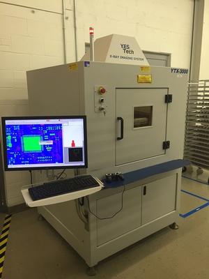
Used SMT Equipment | X-Ray Inspection
Yestech High Resolution Imaging PCB Xray Serial Number: X10706656 Model Number: YTX 3000 Year 2007-2008 130 KV XrayTube with 5 micron spot size Xray on Hours - 18.2 Standby Hours - 328.5 Measured Filament - 2.22 Hamamatsu L19181-02 Sam
Industry News | 2003-02-24 09:32:24.0
Now available with an easy-to-use dispensing gun, Electrolube TCR is a single-component, highly thermally conductive RTV sealant.
Industry News | 2003-03-21 08:12:24.0
Tecan reckons it is consistently producing what may be regarded as the most efficient stencils in the world today.

Parts & Supplies | Pick and Place/Feeders
The definition of SMT SMT is the surface assembly technology,surface mount technology(surface mount technology)(Surface Mounted Technology abbreviation),is currently the most popular electronic assembly industry,a technology and technology. What a
_11.jpg)
Parts & Supplies | Pick and Place/Feeders
Size comparison table for JUKI 500-508 nozzle model KE2010——2040 PART No. PART NAME SIZE(mm) REMARKS E3608-729-0A0 #500 ASS'Y(2-HOLES) 0.5/1.0 E3600-729-0A0 #501 ASS'Y Φ0.7/Φ0.2 E3601-729-0A0 #502 AS
Technical Library | 2023-08-16 18:48:50.0
One of our aerospace customers was looking to automate a few manual operations and asked for suggestions. This customer specializes in assemblies for inflight connectivity for commercial airlines and low orbit satellites. The dispensing process included the application of bonding to the sides of large and small components (4-axis) and the ability to cope with the changing viscosity during processing. The material used was EC-2216 B/A Two Part Epoxy and the largest board size was 12"x10"
Technical Library | 2007-01-31 15:17:04.0
The goal of this project is to evaluate the reliability of lead-free BGA solder joints with a variety of different pad sizes using several different BGA rework methods. These methods included BGAs reworked with both flux only and solder paste attachment techniques and with or without the use of the BEST stay in place StencilQuick™. The daisy chained test boards were placed into a thermal test chamber and cycled between -25ºC to 125ºC over a 30 minute cycle with a 30 minute dwell on each end of the cycle. Each BGA on the board was wired and the continuity assessed during the 1000 cycles the test samples were in the chamber.

www.unisoft-cim.com/pcbtest.htm - In minutes the Unisoft ProntoTEST-FIXTURE software translates CAD & BOM files into real reference designators, netlists, X/Y component pin geometries, values, tolerances, part numbers, etc. This data is used by Test

The PCB Footprint Expert is a powerful CAD library development tool powered by our own proprietary CAD LEAP Technology (Libraries Enhanced with Automated Preferences). It is packed with very powerful advanced library management features that cuts foo
Training Courses | | | IPC-7711/7721 Specialist (CIS)
The Certified IPC-7711/7721 Specialist (CIS) training focuses on rework of electronic assemblies and repair and modification of printed boards and electronic assemblies.
Training Courses | | | IPC-7711/7721 Trainer (CIT)
The Certified IPC-7711/7721 Trainer (CIT) courses recognize individuals as qualified trainers in the area of rework and repair of printed boards and electronic assemblies and prepares them to deliver Certified IPC-7711/7721 (CIS) training.
Events Calendar | Mon Apr 23 00:00:00 EDT 2018 - Thu Apr 26 00:00:00 EDT 2018 | Shanghai, China
SMTA China East Conference 2018
Events Calendar | Wed May 31 00:00:00 EDT 2023 - Wed May 31 00:00:00 EDT 2023 | Holtsville, New York USA
Long Island Chapter Meeting: Fine Feature Paste Printing, Stencil Design and Solder Technology
Career Center | Brooklyn, New York USA | Engineering,Production
Mini-Circuits designs, manufactures and distributes integrated circuits, modules, and sub-systems for high performance radio frequency (RF) and microwave applications. With design, sales and manufacturing locations in over 30 countries, Mini-Ci
Career Center | Brookfield, Wisconsin USA | Engineering
ELECTRONICS MANUFACTURING ENGINEER Salary $50 to 65k Company: Our client is a manufacturer of electronic controls used in a wide variety of industrial and consumer uses. This organization has seen some very strong growth lately, sales have double
SMT Express, Volume 2, Issue No. 9 - from SMTnet.com Volume 2, Issue No. 9 Thursday, September 14, 2000 Featured Article Return to Front Page Book Review Reviewed by Dave Fish (davef ), Pandion Electronics, Inc Title: Wire Bonding
ASYMTEK Products | Nordson Electronics Solutions | https://www.nordson.com/en/divisions/dage/test-types/first-bond-ball-pull-stud-bump-pull?con=t&page=14
. First bond ball pull utilises cold bump pull jaw technology to apply a vertical load (a pull test) to ball bonds and stud bumps. Ball shear tests can sometimes promote pad cratering due to the aggressive nature of the bonding process which can weaken the ball bonds
ORION Industries | http://orionindustries.com/pdfs/gappad.pdf
. * Graphs and data generated from Young's Modulus, calculated using 0.01 inch/min. step rate of strain with a sample size of 0.79 inch2. MODULUS * The modulus of Gap Pad VO is rate dependent due to its viscoelastic properties


