Industry Directory | Consultant / Service Provider / Manufacturer / Other
ScanCAD is an industry leader in inspection, measurement, process control and reverse engineering. Our solutions support OEM's, manufacturers, stencil fabricators, repair depots, and others in optimizing quality and yield.
Industry Directory | Manufacturer
Nepes offers flip chip solutions ranging from wafer bumping to advanced packaging and testing for IC manufactures, module electronics and end-product makers.

New Equipment | Soldering Robots
Applications: 1. Adopt ACF technics to connect TAB/FPC onto TFT/ LCD. 2. Adopt soft soldering technics to connect FPC,FFC onto PCB: Connect single core axes onto plugs. 3. Applied to seal LCD modules in cell phones, electronic translators, PDA,
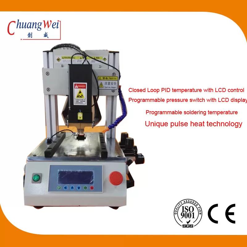
New Equipment | Soldering Robots
Description: Hot bar soldering is extremely effective in bonding components and parts that are dissimilar and difficult to unite. Several examples are listed above, but there are many other soldering situations that call hot bar reflow soldering sys
Electronics Forum | Mon May 07 15:13:03 EDT 2001 | jdtpfacreate
Singh, The equipment varies in price. We make a wire bonder called the HW27U-H Wire Bonder. This is a gold to gold wire ball bonder. The substrate size you mention is within the area we can take into the machine. The key is the bonding area.
Electronics Forum | Tue Jun 14 18:26:32 EDT 2005 | GS
You can find useful informations also on last review of IPC-7085 : Design and Assembly Process Implementation for BGA. Regards GS

Used SMT Equipment | X-Ray Inspection
Very Nice Nicolet Xray Machine For Sale The system is complete and in good working condition See attached pictures and information below Nicolet Imaging Systems Model Number: NXR-1500 Serial Number: 0150011 Year 2000 Variable Speed Joystick
Used SMT Equipment | SPI / Solder Paste Inspection
Vintage: 2008 Description: 3D Solder Paste Inspection Details: • 3D sensing system w/ built-in fiducial camera and lighting • MicroPad Sensor • Mechanical board stop • Auto-width adjust conveyor • Max PCB width: 20” x 20” • Max inspection
Industry News | 2003-03-21 08:12:24.0
Tecan reckons it is consistently producing what may be regarded as the most efficient stencils in the world today.
Industry News | 2018-10-18 08:00:40.0
SMT solder joint quality and appearance inspection process
Parts & Supplies | Pick and Place/Feeders
SMT basic process components include: silk screen (or dispensing), placement (curing), reflow soldering, cleaning, testing, repair 1, silk screen: its role is to paste or patch solder paste printed on the PCB pad, the components f

Parts & Supplies | Pick and Place/Feeders
The definition of SMT SMT is the surface assembly technology,surface mount technology(surface mount technology)(Surface Mounted Technology abbreviation),is currently the most popular electronic assembly industry,a technology and technology. What a
Technical Library | 2023-08-16 18:48:50.0
One of our aerospace customers was looking to automate a few manual operations and asked for suggestions. This customer specializes in assemblies for inflight connectivity for commercial airlines and low orbit satellites. The dispensing process included the application of bonding to the sides of large and small components (4-axis) and the ability to cope with the changing viscosity during processing. The material used was EC-2216 B/A Two Part Epoxy and the largest board size was 12"x10"
Technical Library | 2020-08-27 01:22:45.0
Initially adopted internal specifications for acceptance of printed circuit boards (PCBs) used for wire bonding was that there were no nodules or scratches allowed on the wirebond pads when inspected under 20X magnification. The nodules and scratches were not defined by measurable dimensions and were considered to be unacceptable if there was any sign of a visual blemish on wire-bondable features. Analysis of the yield at a PCB manufacturer monitored monthly for over two years indicated that the target yield could not be achieved, and the main reasons for yield loss were due to nodules and scratches on the wirebonding pads. The PCB manufacturer attempted to eliminate nodules and scratches. First, a light-scrubbing step was added after electroless copper plating to remove any co-deposited fine particles that acted as a seed for nodules at the time of copper plating. Then, the electrolytic copper plating tank was emptied, fully cleaned, and filtered to eliminate the possibility of co-deposited particles in the electroplating process. Both actions greatly reduced the density of the nodules but did not fully eliminate them. Even though there was only one nodule on any wire-bonding pad, the board was still considered a reject. To reduce scratches on wirebonding pads, the PCB manufacturer utilized foam trays after routing the boards so that they did not make direct contact with other boards. This action significantly reduced the scratches on wire-bonding pads, even though some isolated scratches still appeared from time to time, which caused the boards to be rejected. Even with these significant improvements, the target yield remained unachievable. Another approach was then taken to consider if wire bonding could be successfully performed over nodules and scratches and if there was a dimensional threshold where wire bonding could be successful. A gold ball bonding process called either stand-off-stitch bonding (SSB) or ball-stitch-on-ball bonding (BSOB) was used to determine the effects of nodules and scratches on wire bonds. The dimension of nodules, including height, and the size of scratches, including width, were measured before wire bonding. Wire bonding was then performed directly on various sizes of nodules and scratches on the bonding pad, and the evaluation of wire bonds was conducted using wire pull tests before and after reliability testing. Based on the results of the wire-bonding evaluation, the internal specification for nodules and scratches for wirebondable PCBs was modified to allow nodules and scratches with a certain height and a width limitation compared to initially adopted internal specifications of no nodules and no scratches. Such an approach resulted in improved yield at the PCB manufacturer.

www.unisoft-cim.com/pcbtest.htm - In minutes the Unisoft ProntoTEST-FIXTURE software translates CAD & BOM files into real reference designators, netlists, X/Y component pin geometries, values, tolerances, part numbers, etc. This data is used by Test

ACI Technologies Inc. (ACI) is a scientific research corporation dedicated to the advancement of electronics manufacturing processes and materials for The Department of Defense and industry. This video provides an overview of our commercial service
Training Courses | | | PCB Assembly Courses
The PCB assembly courses provide knowledge of different processes and equipment used in TH and SMT assembly of printed circuit boards.
Events Calendar | Mon Apr 23 00:00:00 EDT 2018 - Thu Apr 26 00:00:00 EDT 2018 | Shanghai, China
SMTA China East Conference 2018
Events Calendar | Mon Apr 12 00:00:00 EDT 2021 - Mon Apr 12 00:00:00 EDT 2021 | ,
Europe Chapter Webinar: Tombstoning Components during Reflow Soldering - Causes & Cures
Career Center | Brooklyn, New York USA | Engineering,Production
Mini-Circuits designs, manufactures and distributes integrated circuits, modules, and sub-systems for high performance radio frequency (RF) and microwave applications. With design, sales and manufacturing locations in over 30 countries, Mini-Ci
Career Center | Brookfield, Wisconsin USA | Engineering
ELECTRONICS MANUFACTURING ENGINEER Salary $50 to 65k Company: Our client is a manufacturer of electronic controls used in a wide variety of industrial and consumer uses. This organization has seen some very strong growth lately, sales have double
SMT Express, Volume 2, Issue No. 9 - from SMTnet.com Volume 2, Issue No. 9 Thursday, September 14, 2000 Featured Article Return to Front Page Book Review Reviewed by Dave Fish (davef ), Pandion Electronics, Inc Title: Wire Bonding
ASYMTEK Products | Nordson Electronics Solutions | https://www.nordson.com/en/products/adhesive-dispensing-systems-products/process-air-control-kit
Simplifies setup with compact size, easy-to-use controls and detailed calibration instructions Resources & Downloads Brochures & Data Sheets Process Air Control Kit Global Headquarters 28601 Clemens Road Westlake, Ohio 44145-4551 United States Phone: +1 440.892.1580 Nasdaq
| https://www.eptac.com/ask/gold-wire-bond-failing-pull-test/
) Wire break at neckdown point (reduction of cross section due to bonding process). (a-2) Wire break at point other than neckdown. (a-3) Failure in bond (interface between wire and metallization


