Industry Directory | Manufacturer
Industrial Sensor Vision International specializes in advanced camera technology of high resolution fast speed cameras for automation, AOI, 2-D/3-D, SPI inspection and wafer inspection.
Industry Directory | Other / Consultant / Service Provider / Manufacturer
ScanCAD is an industry leader in inspection, measurement, process control and reverse engineering. Our solutions support OEM's, manufacturers, stencil fabricators, repair depots, and others in optimizing quality and yield.
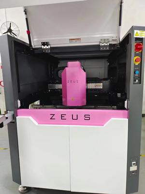
New Equipment | Assembly Services
BEST can provide you with analysis services for your BGAs using x-ray equipment. We rework thousands of BGAs and POPs every year, therefore, we have the expertise in BGA X-ray inspection. BEST can be your outsourced BGA x-ray inspection source for o
New Equipment | Rework & Repair Equipment
BEST HotDots™ are designed to simply and cleanly attach jumper wires on a board. HotDots™ are built to survive at high temperature as both the adhesive and the polyimide material are designed to withstand wash and reflow temperatures. HotDots™ are a
Used SMT Equipment | AOI / Automated Optical Inspection
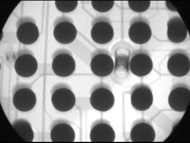
3D Wafer Bump &Wire Bonding AOI Inspection system Highest quality 3D Wire-Inspection. With high-resolution, complete inspection is possible even for Foot-shape. Inspect Mirror-surface without Reflection problem. As for PEMTRON'S unique optical techn
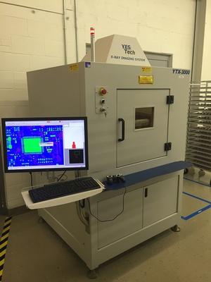
Used SMT Equipment | X-Ray Inspection
Yestech High Resolution Imaging PCB Xray Serial Number: X10706656 Model Number: YTX 3000 Year 2007-2008 130 KV XrayTube with 5 micron spot size Xray on Hours - 18.2 Standby Hours - 328.5 Measured Filament - 2.22 Hamamatsu L19181-02 Sam
Industry News | 2009-07-22 10:45:59.0
BEST Appoints Japanese Distributor
Industry News | 2003-04-17 08:15:33.0
In launching the LA35 series, SMAC reckons it has produced an actuator with unrivalled versatility.
Technical Library | 2020-08-27 01:22:45.0
Initially adopted internal specifications for acceptance of printed circuit boards (PCBs) used for wire bonding was that there were no nodules or scratches allowed on the wirebond pads when inspected under 20X magnification. The nodules and scratches were not defined by measurable dimensions and were considered to be unacceptable if there was any sign of a visual blemish on wire-bondable features. Analysis of the yield at a PCB manufacturer monitored monthly for over two years indicated that the target yield could not be achieved, and the main reasons for yield loss were due to nodules and scratches on the wirebonding pads. The PCB manufacturer attempted to eliminate nodules and scratches. First, a light-scrubbing step was added after electroless copper plating to remove any co-deposited fine particles that acted as a seed for nodules at the time of copper plating. Then, the electrolytic copper plating tank was emptied, fully cleaned, and filtered to eliminate the possibility of co-deposited particles in the electroplating process. Both actions greatly reduced the density of the nodules but did not fully eliminate them. Even though there was only one nodule on any wire-bonding pad, the board was still considered a reject. To reduce scratches on wirebonding pads, the PCB manufacturer utilized foam trays after routing the boards so that they did not make direct contact with other boards. This action significantly reduced the scratches on wire-bonding pads, even though some isolated scratches still appeared from time to time, which caused the boards to be rejected. Even with these significant improvements, the target yield remained unachievable. Another approach was then taken to consider if wire bonding could be successfully performed over nodules and scratches and if there was a dimensional threshold where wire bonding could be successful. A gold ball bonding process called either stand-off-stitch bonding (SSB) or ball-stitch-on-ball bonding (BSOB) was used to determine the effects of nodules and scratches on wire bonds. The dimension of nodules, including height, and the size of scratches, including width, were measured before wire bonding. Wire bonding was then performed directly on various sizes of nodules and scratches on the bonding pad, and the evaluation of wire bonds was conducted using wire pull tests before and after reliability testing. Based on the results of the wire-bonding evaluation, the internal specification for nodules and scratches for wirebondable PCBs was modified to allow nodules and scratches with a certain height and a width limitation compared to initially adopted internal specifications of no nodules and no scratches. Such an approach resulted in improved yield at the PCB manufacturer.
Technical Library | 2016-08-24 06:15:35.0
From consumer electronics to systems control, automotive technology to aviation and aerospace – today, electronics are absolutely essential in many sectors. They increasingly replace mechanical components, eliminating wear and tear and thereby extending the service life. What is easily forgotten in this regard is that electronics are also subject to the laws of mechanics. Mechanical test equipment is crucial to test components for the secure hold of welded, soldered or adhesive bonds. A new, mechanically intricate test probe with universal clamping jaws, that can even grasp the individual bonding wires, is in line with the trend toward ever smaller components. Serving as an actuator for these is a micro drive that can be precisely controlled using a miniaturised motion controller to relieve the control unit in the test device.
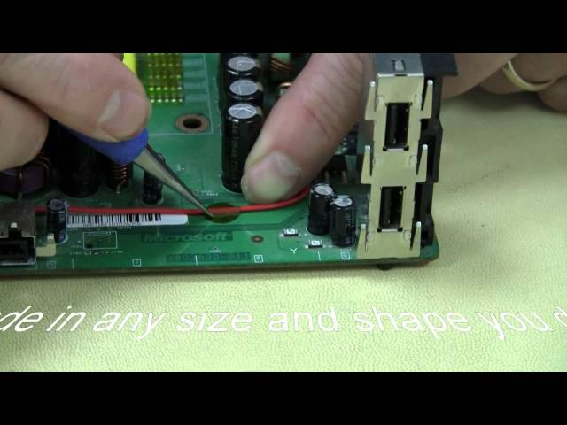
This video demonstrated the use of BEST Inc HotDots(TM) which allow wires to be affixed to the PCB or other surfaces-even when those surfaces go through reflow. There are other similar products out there but none of which can be readily customized no
Training Courses | | | Other Courses
Other courses related to electronics manufacturing and assembly
Training Courses | | | IPC-7711/7721 Specialist (CIS)
The Certified IPC-7711/7721 Specialist (CIS) training focuses on rework of electronic assemblies and repair and modification of printed boards and electronic assemblies.
Career Center | San Diego, California USA | Engineering
MeltroniX is a supplir of MCM/hybrids for the military and space market. We are seeking a process engineer with expertise in wire bonding, including ultrasonic and thermocompession technology.
Career Center | , British Columbia Canada | Engineering
Looking for an engineer or technician to do some contract work on the assembly, testing, and failure of analysis of microelectronics packagages. The individual needs to understand the process of gold wire bonding and eutectic die attachment. Knowle
Career Center | Littleton, CO USA | Production
Possess 18 years relevant work experience in manual/Auto bonding on Micro-Electronic & RF to support new product development in R&D Lab in defense & commercial sectors. Have an advanced soldering skill in both Through-Hole/SMT, and J-STD-001 cert
Career Center | Folsom, California USA | Engineering,Production
A skilled electronics industry worker with experience in solder assembly, rework, and wire-bond. Accustomed to working in both production and engineering envrionments on commercial and military products.
SMT Express, Volume 2, Issue No. 9 - from SMTnet.com Volume 2, Issue No. 9 Thursday, September 14, 2000 Featured Article Return to Front Page Book Review Reviewed by Dave Fish (davef ), Pandion Electronics, Inc Title: Wire Bonding
Surface Mount Technology Association (SMTA) | https://www.smta.org/knowledge/proceedings_abstract.cfm?PROC_ID=5495
Wire-Bonding Reliability of Electroless Ni/Pd/Au Plating - Influence of Electroless Pd Deposition Reaction 中文 MEMBERS LOGIN Membership Become a Member
ASYMTEK Products | Nordson Electronics Solutions | https://www.nordson.com/en/divisions/asymtek/applications/bonding?con=t&page=3
Bonding | Nordson ASYMTEK ASYMTEK Products Corporate | Global Directory | Languages Division Only All of Nordson Fluid Dispensing Systems Jets