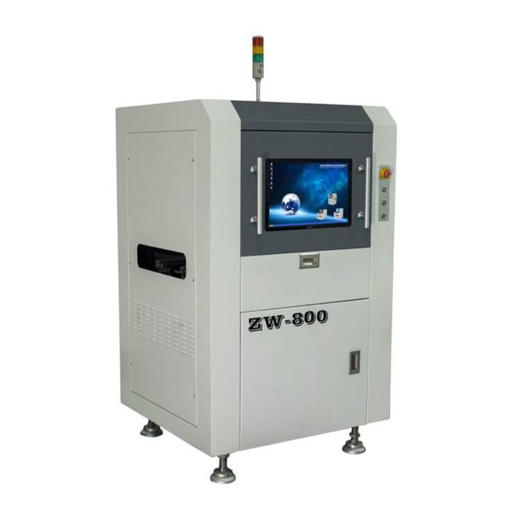
http://www.flason-smt.com/product/SMT-AOI-Machine.html SMT AOI Machine ZW 800 Inspection Component: 0201 chip PCB size::25x25-480*330mm Dimension:980*1080*1410 mm Weight: 600kg Product description: SMT AOI Machine ZW 800 INQUIRY
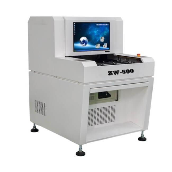
SMT Offline AOI Inspection Machine ZW 500 Dimension:900*1100*1350 mm PCB width:30x30-450x330mm Inspection Component: 0402 chip Weight:Aprox. 450kg Product description: SMT Offline AOI Inspection Machine ZW 500 INQUIRY SMT Offline
Industry News | 2018-10-18 08:00:40.0
SMT solder joint quality and appearance inspection process
Industry News | 2018-10-18 08:01:00.0
SMT solder joint quality and appearance inspection process
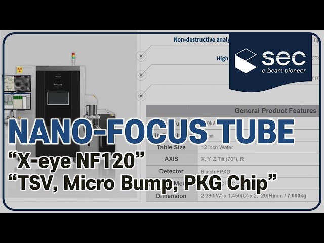
#Xray#Inspection#SEC Nano-focus Tube of 200 nano resolution which is specialized for sub-micron defects of Semiconductor Packaging, Wafer Level Packaging(WLP). -Non-destructive Analysis System -High-Resolution Image with Dual Type CTs -Application
Covering the industrial chain of power semiconductor materials, chips, modules, equipment and other industries, dozens of enterprises from home and abroad participated in the exhibition. This series of products can control the welding cavity rate of
Training Courses | | | IPC-7711/7721 Specialist (CIS)
The Certified IPC-7711/7721 Specialist (CIS) training focuses on rework of electronic assemblies and repair and modification of printed boards and electronic assemblies.
ASYMTEK Products | Nordson Electronics Solutions | https://www.nordson.com/en/divisions/sonoscan/support/application-notes/2466-multiple-voids
About Us Sonoscan Leadership Company History Locations Patent List News Events Careers Nordson SONOSCAN Home Support Application Notes MULTIPLE VOIDS MULTIPLE VOIDS Flip Chip Underfill Multiple Voids
| https://www.eptac.com/faqs/ask-helena-leo/ask/gold-wire-bond-failing-pull-test
) Conductor lifted from board or substrate. (b-5) Fracture within board or substrate. c. For flip-chip configurations: (c-1) Failure in the bond material or pedestal, if applicable. (c-2) Fracture of die (or carrier) or substrate