New Equipment | Education/Training
Bob Willis has an extensive range of training videos available online. The complete video collection is available to view online for a fixed fee, based on a six month period. After purchase you are provided with links to each of the online videos for
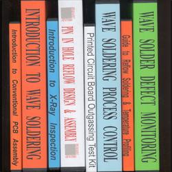
New Equipment | Wave Soldering
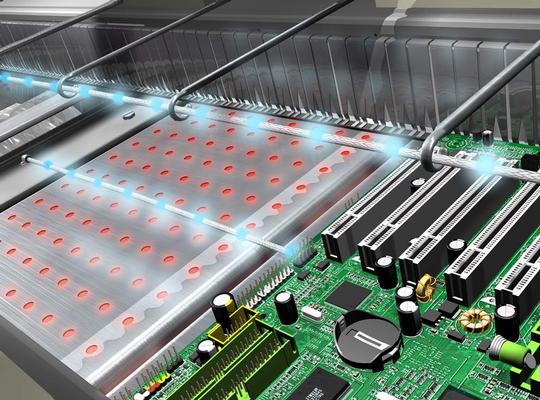
Automatic Profiling, SPC and Traceability for Wave Solder The KIC 24/7 Wave brings an innovative level of automation to the wave solder process: around-the-clock monitoring, SPC charting, analysis, documentation, and production traceability - ALL in
Electronics Forum | Fri Mar 07 04:25:29 EST 2008 | mun4o
Hi, i try to collect data for solder wave process defects, but I dont know how I must calculate these data.Can anyone help me - may be there nave some free software for this.I want to calculate how many ppm is our deffects.And, how is acceptable ran
Electronics Forum | Fri Mar 07 10:55:51 EST 2008 | slthomas
Not sure if you need help with the calculations or the application, so from the beginning: d=defective parts, p=number of parts, dpm=defects per million parts In a nutshell, d/p=dpm/1000000, so dpm=d/p*1000000 We use dpmo (defects per million op
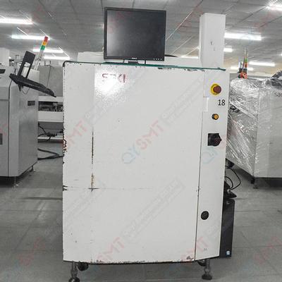
Used SMT Equipment | AOI / Automated Optical Inspection
Saki BF-Frontier AOI System Model BF-Frontier Vintage: 12/2006 Board Thickness: 0.6 - 2.5mm, 24 - 100mils Board Warp: +/-2mm, 79mils PCB Clearance; Top: 40mm, 1.57in Bottom: 40mm, 1.57in Inspection Categories: Presence/Absence, Misalignment, Tomb sto
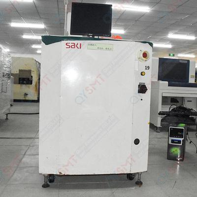
Industry News | 2003-05-22 08:54:17.0
Allows PCA Manufacturers to Compare Costs of Alternative Test Strategies
Industry News | 2003-05-02 08:49:07.0
Group to Assemble Data by Package and Technology Type
Technical Library | 2023-08-02 18:18:23.0
As six sigma (6) and better processes are demanded for higher yields and as organizations move from measuring defects in terms of parts-per-million (ppm) towards parts-per-billion (ppb), the resolution of extant control charts is becoming insufficient to monitor process quality. This work describes the development of a new statistical process control (SPC) chart that is used to monitor processes in terms of defects-per-billion-opportunities (dpbo). A logical extension of the defects-per-million-opportunities (dpmo) control chart, calculations used to derive the dpbo control limits will be presented and examples of in-control and out-of-control processes will be offered.
Technical Library | 1999-05-07 10:14:57.0
This paper describes a model developed to calculate number of redundant good die per wafer. A block redundancy scheme is used here, where the entire defective memory subarray is replaced by a redundant element. A formula is derived to calculate the amount of improvement expected after redundancy. This improvement is given in terms of the ratio of the overall good die per wafer to the original good die per wafer after considering some key factors.

Electrovert's DwellFlex 4.0 is the first solder nozzle designed specifically with Industry 4.0 automation in mind. The patent pending design enables the length of the wave to be adjusted on-the-fly as variable board types are run through the wave.
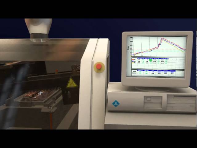
Consistently improve quality and reduce cost with automated profiling, SPC, and traceability for wave solder machines.
Events Calendar | Mon Apr 12 00:00:00 EDT 2021 - Mon Apr 12 00:00:00 EDT 2021 | ,
Europe Chapter Webinar: Tombstoning Components during Reflow Soldering - Causes & Cures
Events Calendar | Wed Mar 07 00:00:00 EST 2018 - Wed Mar 07 00:00:00 EST 2018 | ,
Solder Paste Qualification Testing - SMTA Webinar
Career Center | Regent, North Dakota USA | Management
SUMMARY OF RESPONSIBILITIES: The purpose of this position is to provide guidance and support to production operations in the area of the Manufacturing Supervisors responsibility and to provide a work environment where coworkers have the tools, train
Career Center | Killdeer, North Dakota USA | Technical Support
SUMMARY OF RESPONSIBILITIES Technical collaboration with engineers and operators to explain scientific and technical ideas in language that is easier for average readers to comprehend. The purpose of this position is to provide guidance and suppo
Career Center | chennai, Tamil nadu India | Engineering,Production
KEY SKILLS; 1.PRINTING, PICK AND PLACE MACHINE OPERATION, 2.REFLOW OVEN CHARACTERISTICS, 3.IPC STANDARD,QUALITY POLICIES 4.AOI PROGRAMMING 5.c,c++LANGUAGES. 6.VerilogHDL. 7.ORCAD,PSPICE software known.
Career Center | Theni, Tamilnadu India | Engineering
NPI Engineer: • Playing a role as NPI leader of the Telecom, Aerospace & Server Products to introduce and run to qualify the engineering build from customer. • Conducting Weekly NPI meeting with the CFT team to review the progress of the NPI schedu
GPD Global | https://www.gpd-global.com/co_website/pdf/lead-former/CF8-User-Guide-801-1-07.pdf
. 04/02/07 GPD Global® CF-8 Precision Axial Lead Former 04/02/07 ii Warranty GPD Global® (GPD) warrants that this product will be free from defects in material and workmanship for a period of one (1


winsouce.jpg)
.gif)
