
Industry Directory | Consultant / Service Provider / Equipment Dealer / Broker / Auctions / Manufacturer's Representative / Training Provider
Products, services, training & consulting for the assembly, rework & repair of electronic assemblies. BGA process experts. Manufacturers Rep, Distributor & Service Provider for Seamark/Zhuomao and Shuttle Star BGA Rework Stations.
Online catalog of electronic components from different manufacturers -- component selection tool for electronics engineers
New Equipment | Rework & Repair Equipment
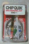
We are a distributor of Chip Quik SMD rework products. Call for pricing or check out our on line store: https://youtu.be/DBJ1MxqD3d0 (888) 406-2830
New Equipment | Solder Materials
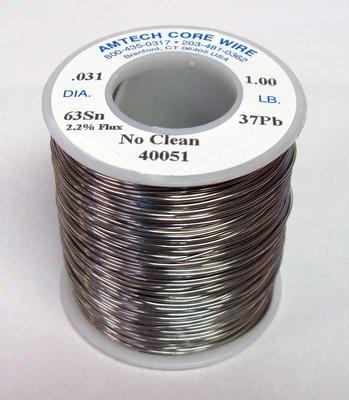
We stock Amtech and Chip Quik wire roll solder in both lead and lead free. Sizes as small as .010" Call (888) 406-2830
Electronics Forum | Tue Feb 27 11:03:09 EST 2007 | Marcin
Hi All, Anybody knows what is the minimum clearance between through hole component and chip component? Problem description: On bottom side of my pcb are only 0603 chip components mounted on glue. One of the component is located very close to hole
Electronics Forum | Wed Feb 28 21:42:56 EST 2007 | davef
Very smart, Chunks.
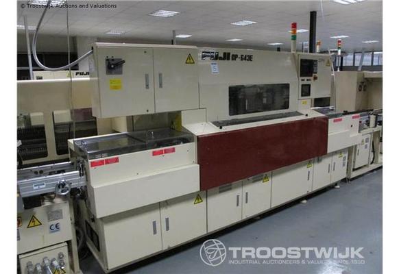
Used SMT Equipment | Chipshooters / Chip Mounters
FUJI, Chip Shooter, type CP643E, s.n. 2066, Left to right, cap. 40.000 CPH, Device input 140-8mm, with 20 heades, 6 nozels each, 2 tables 70 feeders each, PCB dimensions Max: 457mm x 356mm Min: 80mm x 60mm,Board Thickness: 0.3 to 4.0 mm, Component ca
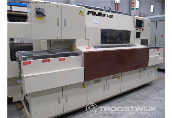
Used SMT Equipment | Chipshooters / Chip Mounters
FUJI, Chip Shooter, type CP643E, s.n. 1278, Left to right, cap. 40.000 CPH, Device input 140-8mm, with 20 heades, 6 nozels each, 2 tables 70 feeders each, PCB dimensions Max: 457mm x 356mm Min: 80mm x 60mm,Board Thickness: 0.3 to 4.0 mm, Component ca
Industry News | 2013-08-15 20:58:22.0
Heller Industries announced today that they have entered into a joint development agreement with International Business Machines Corporation (NYSE: IBM), to collaborate on the development of fluxless mass reflow furnace equipment and process for high volume manufacturing. The fluxless process utilizes gas phase formic acid to replace standard fluxing agents, and eliminates the need for pre-reflow fluxing and post-reflow flux cleanup steps.
Industry News | 2003-06-18 07:56:46.0
The IPC-9850 test materials kit includes all the materials needed for manufacturers to test flexible placement machines and chip shooters to the specifications of the IPC-9850 standard.
Parts & Supplies | Pick and Place/Feeders
Product number: RX - 7 Detailed product introduction Characteristic With high productivity, versatility, highquality new modular placement machine RX 7 listed Component placement speed (best conditions): 75000 CPH chip components Element size: 0
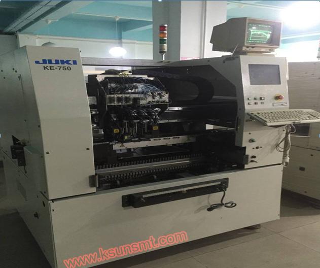
Parts & Supplies | Chipshooters / Chip Mounters
Model :KE-750 Placement speed:14, 400CPH(0.25sec/chip) Component mount range:1.0x0.5mm~□20mm or 23.5x11mm Station:80 Power supply:1P/200V/2.5KVA Size:1,400x1, 410x1, 551mm Weight:1,150kg Currently, all the machines with very good competitive
Technical Library | 2023-01-17 17:22:28.0
The impact of voiding on the solder joint integrity of ball grid arrays (BGAs)/chip scale packages (CSPs) can be a topic of lengthy and energetic discussion. Detailed industry investigations have shown that voids have little effect on solder joint integrity unless they fall into specific location/geometry configurations. These investigations have focused on thermal cycle testing at 0°C-100°C, which is typically used to evaluate commercial electronic products. This paper documents an investigation to determine the impact of voids in BGA and CSP components using thermal cycle testing (-55°C to +125°C) in accordance with the IPC- 9701 specification for tin/lead solder alloys. This temperature range is more typical of military and other high performance product use environments. A proposed BGA void requirement revision for the IPC-JSTD-001 specification will be extracted from the results analysis.
Technical Library | 2023-11-25 07:46:13.0
In the dynamic realm of Surface Mount Technology (SMT), where efficiency and precision are paramount, I.C.T, a renowned SMT equipment manufacturer, proudly unveils its latest innovation – the I.C.T-910 Automatic IC Programming System. Crafted to cater to the intricate demands of SMD chip programming, this cutting-edge device vows to redefine your programming experience and elevate production capabilities. Programming system.png The Power of IC Programming System: As a beacon of excellence in IC Programming Systems, the I.C.T-910 seamlessly integrates advanced technology with user-friendly features. This system empowers manufacturers in the SMT industry, offering versatility in programming needs by accommodating a wide range of SMD chips. Precision Programming: The I.C.T-910 boasts unparalleled precision in programming SMD chips, ensuring accuracy in every generated code. In the SMT industry, where even the slightest error can lead to setbacks, this precision is indispensable. Efficiency Redefined: Accelerate your production timelines with the I.C.T-910's efficient programming capabilities. Engineered to optimize workflows, this system ensures rapid programming without compromising quality, recognizing that time is money in the SMT industry. User-Friendly Interface: Navigating the complexities of IC programming is simplified with the I.C.T-910's intuitive user interface. Operators, even without extensive programming expertise, can harness the system's power, minimizing the learning curve and maximizing productivity. Compatibility and Adaptability: The I.C.T-910 breaks free from limitations, supporting a wide array of SMD chip models. It is a versatile solution for diverse programming requirements, allowing you to stay ahead of technological advancements. Why Choose I.C.T-910 IC Programming System? 8 sets of 32-64sit burners Nozzle: 4pcs Camera: 2pcs (Component camera + Marking camera) UPH: 2000-3000PCS/H Package type: PLCC, JLCC, SOIC, QFP, TQFP, PQFP, VQFP, TSOP, SOP, TSOPII, PSOP, TSSOP, SON, EBGA, FBGA, VFBGA, BGA, CSP, SCSP, and so on. Compatibility: Adapters provided based on customer products. Simple operation interface: Modular and layered interface with pictures and texts for easy operation. System upgrade: Free software upgrade service. Reliability: Trust in the I.C.T-910, a programming system that prioritizes reliability. Rigorous testing ensures consistent and dependable performance, reducing the risk of programming errors and downtime. Elevate Your Competitiveness: Incorporate the I.C.T-910 into your production line to elevate competitiveness in the market. Stay ahead with a programming system designed to meet the demands of the fast-paced SMT industry. Embrace the Future with I.C.T-910: In a landscape where precision, efficiency, and adaptability are non-negotiable, the I.C.T-910 Automatic IC Programming System emerges as the game-changer for SMT manufacturers. Revolutionize your programming processes, enhance productivity, and future-proof your operations with the I.C.T-910. Choose I.C.T-910 and stay ahead in the SMT industry, ushering in the next era of IC programming excellence.

Broader scope, the latest ultra-small SMD components (01005) count, the series is as follows: These are the components package specifications. Functions: 1, Empty chip detection capabilities SMD chip counter, the job is simple, positive and neg
Description MODEL ID: CM402-L MODEL NUMBER: KXF-4Z4C PCB DIMENSIONS: L 50 mm x W 50mm to L 510 mm Ã? W 460 mm HEAD TYPE: Type A-2 (12/12 nozzles HIGH-SPEED) (OPTION) Number of nozzles: 12 nozzles/head Maximum speed: 0.052 s/chip (69,500
Training Courses | | | IPC-7711/7721 Specialist (CIS) Recert.
The Certified IPC-7711/7721 Specialist (CIS) recertification courses are intended for those individuals who were previously certified as IPC-7711/7721 Specialist.
Training Courses | | | IPC-7711/7721 Trainer (CIT)
The Certified IPC-7711/7721 Trainer (CIT) courses recognize individuals as qualified trainers in the area of rework and repair of printed boards and electronic assemblies and prepares them to deliver Certified IPC-7711/7721 (CIS) training.
Events Calendar | Mon Apr 12 00:00:00 EDT 2021 - Mon Apr 12 00:00:00 EDT 2021 | ,
Europe Chapter Webinar: Tombstoning Components during Reflow Soldering - Causes & Cures
Events Calendar | Mon Apr 23 00:00:00 EDT 2018 - Thu Apr 26 00:00:00 EDT 2018 | Shanghai, China
SMTA China East Conference 2018
Career Center | New Delhi, New Delhi India | Sales/Marketing
Equipment related to PCB Assembly ( wave soldering , Selective soldering , reflow , pick'n'place system , PCB Inspection system , PCB Rework System ,Flip - Chip Bonding system , Component forming system ). ---> Equipment relat
Career Center | Middleboro, Massachusetts USA | Production
Highly motivated SMT Repair/ Assembly Operators needed for Contract Electronics Manufacturer. Duties include: repair and soldering of SMT and TH components, assembling of PCB's, and operation of automated production equipment. Experience using vario
Career Center | , Portugal | Engineering,Maintenance,Production,Quality Control,Technical Support
SMT Process engineer Quality Efficiency Continuous improvement 11 years of experience in high volume production in a Japanese corporation Expertise in: Solder paste printing (DEK, Panasonic) Adhesive dispensing (FUJI, Panasonic) Components Pick and p
Career Center | Bangalore-560026, Karnataka India | Engineering,Maintenance,Technical Support
New Product Introduction & Product dovelopment
PCB Libraries, Inc. | https://www.pcblibraries.com/forum/topic551&OB=ASC.html
Chip Component Land Pattern - PCB Libraries Forum Forum Home > Libraries > Footprints / Land Patterns New Posts FAQ Search Events Register Login Chip Component Land Pattern
KingFei SMT Tech | https://www.smtspare-parts.com/sale-11789719-k9f4g08u0d-sib0-samsung-chip-component-assembled-smt-machine-parts.html
K9F4G08U0D-SIB0 Samsung Chip Component Assembled SMT Machine Parts Leave a Message We will call you back soon! Your message must be between 20-3,000 characters


