
SMT256EP solderable adhesive is self-leveling and self-soldering adhesives, which has been designed for high temperature Pb-free application. By comparison with conductive adhesives (Ag), SMT256EP solderable adhesive has higher stable electrical and
New Equipment | Board Handling - Pallets,Carriers,Fixtures
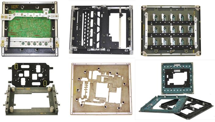
Our Wave Solder Fixtures increase productivity and eliminate defects in your pcb assembly process. This type of fixture supports the pcb on all four sides eliminating warpage that can cause solder skips and bridges or pcb flooding. They also elim
Electronics Forum | Thu Jun 22 11:42:29 EDT 2000 | Chrys Shea
Sal, Silly question: Were the parts skewed before they went into the oven? I've chased down a few similar reflow problems in my lifetime, only to find out it was a pick and place problem. Wrong nozzle size, bad nozzle, feeder not advancing all
Electronics Forum | Thu Sep 11 15:23:31 EDT 2003 | Peter L.
I have come across a rash of failed assemblies that have 0805 capacitors and resistors, bottom side glued, wave soldered and washed. Trouble shooter reported touching up the solder joints on a few areas and the boards would pass test. I had a look a
.jpg)
Used SMT Equipment | Pick and Place/Feeders
FUJI/NXTIIC Used Chip Mounter The Fuji NXT is designed to meet the demands of modern production environments. Its interchangeable placement heads allow each machine module to function as either a high speed chip counter or a multi-function placemen
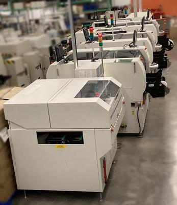
Used SMT Equipment | Turnkey Lines
Functional Pre-Owned Complete SMT Assembly Line - Still Operational (Subject to prior sell, I am listing this on other venues) Up for sale is a full turnkey SMT line and all of it's accessories, of which there are a lot, fe
Industry News | 2011-11-03 21:52:00.0
By davef: I was fortunate to be able to attend the SMTAI Exhibition Oct. 18-19, 2011. While I was walking around looking at the booths and talking to the exhibitors, I got this idea that I would report back on things that I found interesting. You know spread the news, since not everyone was there.
Industry News | 2022-09-26 06:35:13.0
The electronics industry is calling on U.S. President Joe Biden to address urgent industrial base vulnerabilities and deliver on the promise of the CHIPS Act by prioritizing domestic development of printed circuit boards (PCBs) and integrated circuit (IC) substrates under Title III of the Defense Production Act.
Technical Library | 2023-07-25 16:50:02.0
Some of the new handheld communication devices offer real challenges to the paste printing process. Normally, there are very small devices like 01005 chip components as well as 0.3 mm pitch uBGA along with other devices that require higher deposits of solder paste. Surface mount connectors or RF shields with coplanarity issues fall into this category. Aperture sizes for the small devices require a stencil thickness in the 50 to 75 um (2-3 mils) range for effective paste transfer whereas the RF shield and SMT connector would like at least 150 um (6 mils) paste height. Spacing is too small to use normal step stencils. This paper will explore a different type of step stencil for this application; a "Two-Print Stencil Process" step stencil. Here is a brief description of a "Two-Print Stencil Process". A 50 to 75 um (2-3 mils) stencil is used to print solder paste for the 01005, 0.3 mm pitch uBGA and other fine pitch components. While this paste is still wet a second in-line stencil printer is used to print all other components using a second thicker stencil. This second stencil has relief pockets on the contact side of the stencil any paste was printed with the first stencil. Design guidelines for minimum keep-out distances between the relief step, the fine pitch apertures, and the RF Shields apertures as well relief pocket height clearance of the paste printed by the first print stencil will be provided.

The LPKF MicroLine 1000 S is perfect for cutting break-out tabs and complex contours at highest accuracy. The benefits include shorter time to market and much higher quality cuts than conventional methods. The machine's UV laser is an optimal tool fo
Training Courses | | | PCB Assembly Courses
The PCB assembly courses provide knowledge of different processes and equipment used in TH and SMT assembly of printed circuit boards.
Training Courses | | | PCB Assembly Courses
The PCB assembly courses provide knowledge of different processes and equipment used in TH and SMT assembly of printed circuit boards.
Career Center | Bangalore-85, ka India | Production
As a Sr.Technician involved in production activities like programming, taking care of the production, process, rectifying the process problems, constantly getting in touch with the customers for any quality issues & other production activities, invol
Career Center | Thanjavur, India | Production,Quality Control,Technical Support
work in one year and above Quality engineer in sanmina,current work in SMT Technical engineer in coimbatore
INSERT INTO tracking_express (userid, username, page_id, ts) VALUES ('#Quser_profile.id#', '#Quser_profile.username#', 97, (#ts#)) SMT Express, Volume 4, Issue No. 1 - from SMTnet.com Volume 4, Issue No. 1 Thursday, January 17, 2002 Featured
| https://www.eptac.com/ask/ipc-a-610-acceptable-requirements-for-nicks-and-chip-outs/
: In IPC-A-610 section 9.4 on page 9-8 component damage there seems to be a lack of class three acceptable requirements for nicks or chip-outs in ceramic bodied components that are not in the termination area
ASYMTEK Products | Nordson Electronics Solutions | https://www.nordson.com/en/divisions/sonoscan/support/publications
. Microelectronics - Bonded Wafer Microelectronics - Chip Capacitor Microelectronics - Chip Scale Package Microelectronics - Flip Chip Microelectronics - Hybrid/MCM/SIP Microelectronics - IGBT Power

.gif)


