Industry Directory | Manufacturer
Shenzhen Huancheng Automation equipment Co.,ltd (referred to as the "HC"), a High-speed developing enterprise specializing in High Precision Automatic Solder Paste Printer research and development.
Industry Directory | Consultant / Service Provider
PCB assembly services, both US and offshore. We handle basic through-hole to standard surface mount to ultra-fine pitch. Quote and order PCB fabrication and assembly online.
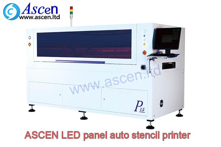
Full AUTO PCB screen printing machine solder paste printers mainly for led tube light PCB large production solutions,Catering to customers’ ultra-long PCB printing demand,Auto pcb stencil printer provides fast, high-precision printing
New Equipment | Cleaning Equipment
SMT PCB Cleaner UC-250M Adhesive roll 2 rolls Width adjustment Manual PCB size 50﹡50~330﹡250 mm Weight About 100 kg Product description: SMT PCB Cleaner UC-250M, Adhesive roll 2 rolls, Width adjustment Manual, PCB size 50﹡50~330﹡250 mm, Weight
Industry News | 2003-03-31 09:51:04.0
The SMTA has formed the SMTA International Technical Committee for 2003.
Industry News | 2003-02-18 09:39:06.0
Encourages You to Submit an Abstract for this Year's Conference
.jpg)
 (8).jpg)
Technical Library | 2020-08-27 01:22:45.0
Initially adopted internal specifications for acceptance of printed circuit boards (PCBs) used for wire bonding was that there were no nodules or scratches allowed on the wirebond pads when inspected under 20X magnification. The nodules and scratches were not defined by measurable dimensions and were considered to be unacceptable if there was any sign of a visual blemish on wire-bondable features. Analysis of the yield at a PCB manufacturer monitored monthly for over two years indicated that the target yield could not be achieved, and the main reasons for yield loss were due to nodules and scratches on the wirebonding pads. The PCB manufacturer attempted to eliminate nodules and scratches. First, a light-scrubbing step was added after electroless copper plating to remove any co-deposited fine particles that acted as a seed for nodules at the time of copper plating. Then, the electrolytic copper plating tank was emptied, fully cleaned, and filtered to eliminate the possibility of co-deposited particles in the electroplating process. Both actions greatly reduced the density of the nodules but did not fully eliminate them. Even though there was only one nodule on any wire-bonding pad, the board was still considered a reject. To reduce scratches on wirebonding pads, the PCB manufacturer utilized foam trays after routing the boards so that they did not make direct contact with other boards. This action significantly reduced the scratches on wire-bonding pads, even though some isolated scratches still appeared from time to time, which caused the boards to be rejected. Even with these significant improvements, the target yield remained unachievable. Another approach was then taken to consider if wire bonding could be successfully performed over nodules and scratches and if there was a dimensional threshold where wire bonding could be successful. A gold ball bonding process called either stand-off-stitch bonding (SSB) or ball-stitch-on-ball bonding (BSOB) was used to determine the effects of nodules and scratches on wire bonds. The dimension of nodules, including height, and the size of scratches, including width, were measured before wire bonding. Wire bonding was then performed directly on various sizes of nodules and scratches on the bonding pad, and the evaluation of wire bonds was conducted using wire pull tests before and after reliability testing. Based on the results of the wire-bonding evaluation, the internal specification for nodules and scratches for wirebondable PCBs was modified to allow nodules and scratches with a certain height and a width limitation compared to initially adopted internal specifications of no nodules and no scratches. Such an approach resulted in improved yield at the PCB manufacturer.
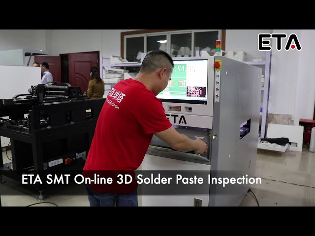
SMT On-line 3D Solder Paste Inspection If you could not find any similar items you want, you may send some photos to us. because our catalog and website haven't included all of our products. solder paste inspection,SMT SPI,SPI machine, SPI in
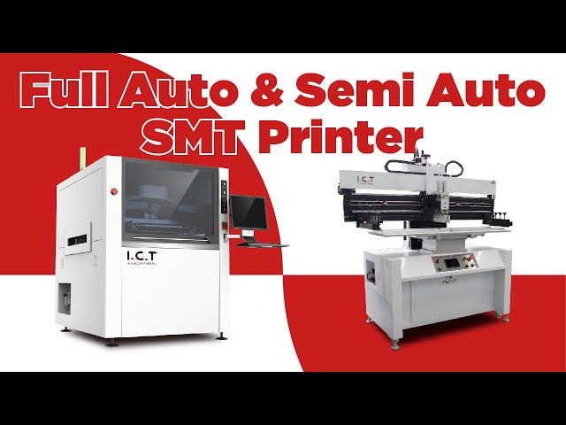
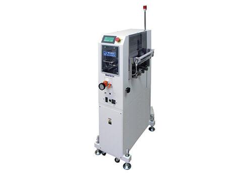
Full-auto SMT Stencil Printer is indispensable equipment in SMT production Line. It is generally composed of board mounting, solder paste, imprinting, and circuit board transfer. Widely used are Full-auto SMT Stencil Printer and semi-auto SMT Stencil
SMT Express, Volume 5, Issue No. 3 - from SMTnet.com Machine Capability Measurement on SMT Equipment by Romain Schmitt, Jean Marie Guillet - Solectron Technology, Inc. Introduction by Michael Sivigny of EAGLE-EYED ONE
| https://www.smtfactory.com/I-C-T-V8-SMT-off-line-Aoi-inspection-machine-For-Pcb-pd48670624.html
I.C.T-V8 | SMT off line Aoi inspection machine For Pcb from China manufacturer - Dongguan Intercontinental Technology Co.,Ltd. English Français Pусский Español Português Deutsch Italiano 日本語 한국어 Tiếng Việt Türk dili Home About Us Company Profile
KingFei SMT Tech | https://www.smtspare-parts.com/supplier-144643p52-smt-spare-parts
SMT Spare Parts factory, Buy good quality SMT Spare Parts products from China Leave a Message We will call you back soon! Your message must be between 20-3,000 characters