Industry Directory | Manufacturer
A manufacturer of desoldering braid (wick) with an emphasis on continuing advancement in soldering/desoldering technology, visual and x-ray inspection systems, fume extraction, and solder paste inspection systems.
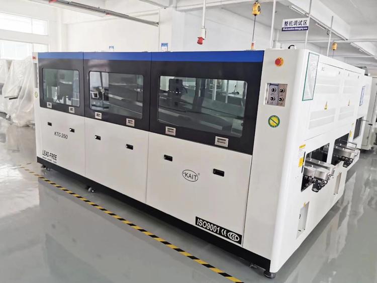
New Equipment | Wave Soldering
Dual Rail Wave Soldering Machine KTU-350D SMT Reflow Oven, Wave Soldering Machine Videos Preheating zone 4 zones Solder pot capacity Approx.480kg Solder pot capacity Approx.480kg Dimension 4500*3000*1730mm Product description: Dual Rail Wave S
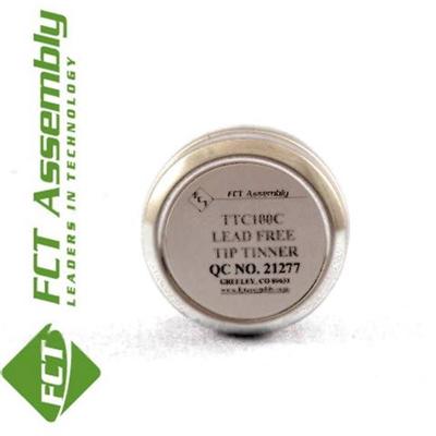
New Equipment | Solder Materials
Tip tinner to aid in cleaning and re-tinning solder iron tips de-wetted by use which can’t be repaired with sponge pads and cored solder wire. Use of TTC100C LEAD FREE Tip Tinner offers the following advantages: Lead Free SN100C tin/copper/nic
Industry News | 2018-10-18 08:55:30.0
Nitrogen Protection Reflow Oven
Industry News | 2018-12-08 03:29:29.0
SMT Dictionary – Surface Mount Technology Acronym and Abbreviation
Technical Library | 2020-08-27 01:22:45.0
Initially adopted internal specifications for acceptance of printed circuit boards (PCBs) used for wire bonding was that there were no nodules or scratches allowed on the wirebond pads when inspected under 20X magnification. The nodules and scratches were not defined by measurable dimensions and were considered to be unacceptable if there was any sign of a visual blemish on wire-bondable features. Analysis of the yield at a PCB manufacturer monitored monthly for over two years indicated that the target yield could not be achieved, and the main reasons for yield loss were due to nodules and scratches on the wirebonding pads. The PCB manufacturer attempted to eliminate nodules and scratches. First, a light-scrubbing step was added after electroless copper plating to remove any co-deposited fine particles that acted as a seed for nodules at the time of copper plating. Then, the electrolytic copper plating tank was emptied, fully cleaned, and filtered to eliminate the possibility of co-deposited particles in the electroplating process. Both actions greatly reduced the density of the nodules but did not fully eliminate them. Even though there was only one nodule on any wire-bonding pad, the board was still considered a reject. To reduce scratches on wirebonding pads, the PCB manufacturer utilized foam trays after routing the boards so that they did not make direct contact with other boards. This action significantly reduced the scratches on wire-bonding pads, even though some isolated scratches still appeared from time to time, which caused the boards to be rejected. Even with these significant improvements, the target yield remained unachievable. Another approach was then taken to consider if wire bonding could be successfully performed over nodules and scratches and if there was a dimensional threshold where wire bonding could be successful. A gold ball bonding process called either stand-off-stitch bonding (SSB) or ball-stitch-on-ball bonding (BSOB) was used to determine the effects of nodules and scratches on wire bonds. The dimension of nodules, including height, and the size of scratches, including width, were measured before wire bonding. Wire bonding was then performed directly on various sizes of nodules and scratches on the bonding pad, and the evaluation of wire bonds was conducted using wire pull tests before and after reliability testing. Based on the results of the wire-bonding evaluation, the internal specification for nodules and scratches for wirebondable PCBs was modified to allow nodules and scratches with a certain height and a width limitation compared to initially adopted internal specifications of no nodules and no scratches. Such an approach resulted in improved yield at the PCB manufacturer.
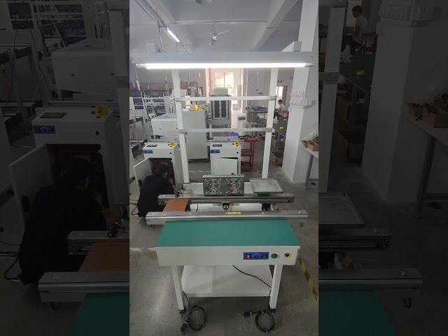
Soldering PCB Rework Conveyor 1. Modular design 2. Weighted design improves stability 3. Smooth and parallel width adjustment (screw) 4. PCB detection mode 5. Customizable equipment length 6. Adjustable transport speed 7. SMEMA 8. Motor drive 9. Hig
Soldering PCB Rework Conveyor 1. Modular design 2. Weighted design improves stability 3. Smooth and parallel width adjustment (screw) 4. PCB detection mode 5. Customizable equipment length 6. Adjustable transport speed 7. SMEMA 8. Motor drive 9. Hig
Career Center | NORTHRIDGE, California USA | Engineering
EDUCATION BS Electronics and Communication Engineering Gujarat University MS Electrical Engineering California State University, Northridge ACADAMIC PROJECT Fabrication and Characterization of Silicon Carbide (SiC) MESFE
GPD Global | https://www.gpd-global.com/co_website/features-needlecleaner.php
. Automatic Nozzle Cleaning. Wipe Styles Needle Cleaner tool-less design makes changing wipes very easy. Simply remove magnetic pad holders, remove old pads, and insert new ones
| https://pcbasupplies.com/stencil-cleaning-paper/
Stencil Printers ezLOAD 40 Pads and Accessories Pick-and-Place ezLOAD Flex ezLOAD Replacment Pads Stencil Cleaning Paper Dry Storage Cabinets Shop By Brand Count On Tools Thermaltronics BEAU TECH Southern


