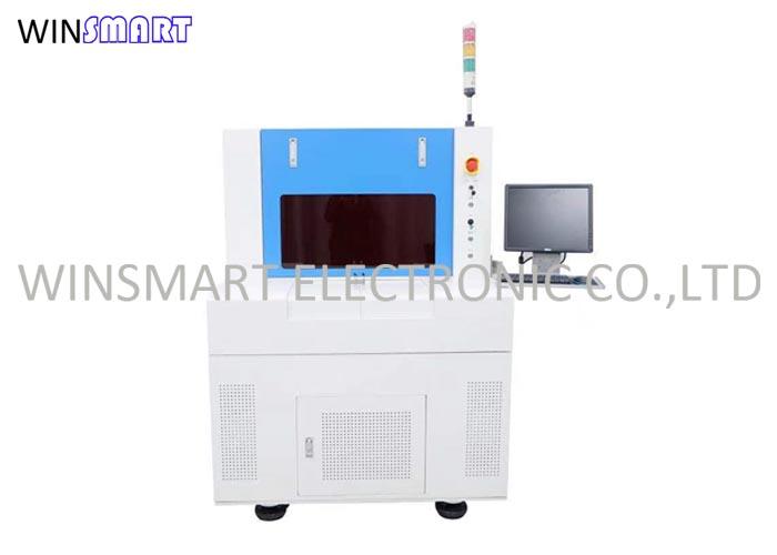
15W UV Laser Economic PCB Laser Depaneling System PCB Laser Depaneling System Specification: Laser solid-state UV laser Laser Wavelength 355nm Laser Source UV 15W@30KHz Positioning Precision ±2μm
UV Laser PCB Depaneling System, Dual Table for High Volume Laser Depaneling Purpose: The processing and application objects are PCB, FPC soft and hard plate and related material cutting, cover opening and other operations. Efficient integration
Electronics Forum | Fri Aug 22 03:19:08 EDT 2008 | andrzej
Hi, what do you mean by collapsed ? Can you describe or send a photo ?
Electronics Forum | Mon Jul 12 09:13:08 EDT 1999 | Mark Charlton
I need some advice concerning reflow of a BGA-292. Since I am not ready to change my entire process to no-clean, I decided to place the lone BGA-292 on a proto run using our BGA re-work station. The pcb is a moderately dense, single-sided, 8-layer
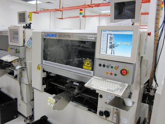
Used SMT Equipment | Pick and Place/Feeders
Dear Customer, We have the machine as below for sales, Model: KE 2070 L Vintage: 2010 No Feeder Please contact us if you are interested. Regards Michael var LEO_HIGHLIGHTS_INFINITE_
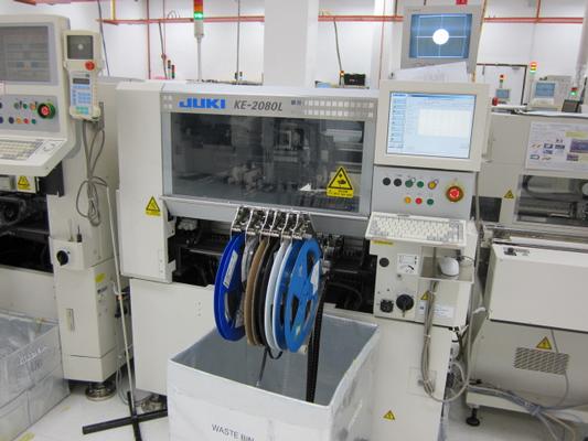
Used SMT Equipment | Pick and Place/Feeders
Dear Customer, We have the following machine for sales, Model: KE 2080 L Vintage: 2010 No Feeder C/W Tray unit Please contact us if you are interested. Regards Michael var LEO
Industry News | 2002-03-29 07:49:10.0
A Corporate Workforce Reduction of 25%
Industry News | 2020-05-28 10:52:31.0
SFI High Attenuation Frameless Enclosures are compact, easy to setup and tear down, and offer excellent EMI isolation on the benchtop
Technical Library | 2023-12-15 03:06:24.0
The first process in the SMT industry is solder paste printing. After the solder paste printing is completed, electronic components are attached to PCB pads through a SMT machine, and then reflow soldered. A preliminary PCB board is roughly processed. SMT is a combination of multiple devices, and such a line is called an SMT production line. Our common PCBA is processed through this process. In SMT technology, each process is very important, and poor quality can be caused by different process defects. Today, we are discussing the causes and countermeasures of SMT printing collapse.
Technical Library | 2019-05-21 17:38:55.0
Last month we presented Flip Chip Rework.As promised, this month we follow up with attachment techniques. Flip chip assembly is a key technology for advanced packaging of microelectronic circuits. It allows attachment of a bare chip to a packaging substrate in a face-down configuration, with electrical connections between the chip and substrate via conducting “bumps.” Flip chip technology was first invented by IBM for mainframe computer application in the early 1960s. Semiconductor devices are mounted face down and electrically and mechanically connected to a substrate (Figure 1). IBM called this manufacturing process a C4 process (controlled collapse chip connection).
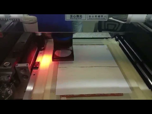
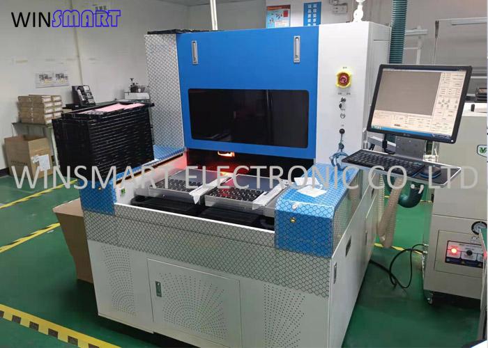
15W UV Laser Economic PCB Laser Depaneling System PCB Laser Depaneling System Specification: Laser solid-state UV laser Laser Wavelength 355nm Laser Source UV 15W@30KHz Positioning Precision ±2μm
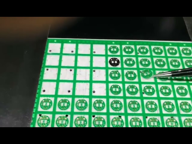
UV Laser PCB Depaneling System, Dual Table for High Volume Laser Depaneling Purpose: The processing and application objects are PCB, FPC soft and hard plate and related material cutting, cover opening and other operations. Efficient integration
| https://www.eptac.com/wp-content/uploads/2021/11/webinar_eptac_09_16_09.pdf
. The control panel contains three panes that can be expanded or collapsed by clicking the arrow on the left side of each pane. To Leave a Webinar: 1. From the Attendee Control Panel File Menu, select Exit
46969 | http://hellerindustries.com/wp-content/themes/hellerIndustries/js/vendor_scripts.js?ver=1.0.1
Heller Industries Inc.


