Industry Directory | Consultant / Service Provider
A leading company in the fields of engineering, procurement and testing of high reliability components and electronic equipment within the space and other high reliability markets.
Military, Space, Aerospace and Industrial component design, assembly and test facility.

New Equipment | Curing Equipment
Heller 788 In-line, Continuous Cure, Vertical Format Oven This elevator format oven utilizes vertical space to accomodate curing applications of up to 4 hours while only occupying 96" (2.5m) of floorspace. Perfect for underfill and encapsulant.
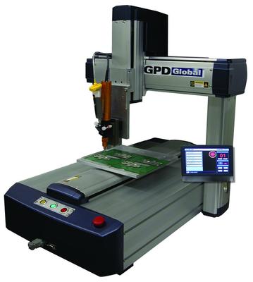
Simplify Dispensing with GPD Global’s Island Series Dispense Platforms Island Series robots give you versatility to do simple, repetitive automation jobs. Work areas range from 300 mm x 400 mm to 400 mm x 400 mm. All Island Series robots are compati

Used SMT Equipment | Chipshooters / Chip Mounters
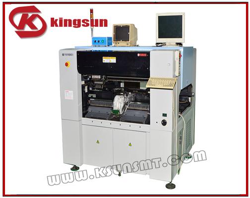
Product name: YV100 Ⅱ YAMAHA multi-functional SMT machine Product number: YV100 Ⅱ Products in detail YAMAHA multi-function placement machine YAMAHA YV100II The brand YAMAHA model YV100 - II Automatic manual automatic SMT speed 10000 (grain per
Used SMT Equipment | SMT Equipment
Product name: YV100 Ⅱ YAMAHA multi-functional SMT machine Product number: YV100 Ⅱ Products in detail YAMAHA multi-function placement machine YAMAHA YV100II The brand YAMAHA model YV100 - II Automatic manual automatic SMT speed 10000 (grain per
Industry News | 2016-04-20 10:27:40.0
BEST, Inc. was presented Circuit Assembly’s NPI Award for its HeatShield Gel™ high temperature shielding product at the IPC APEX Expo on Feb. 24 in San Diego, Calif.
Industry News | 2016-01-05 16:10:10.0
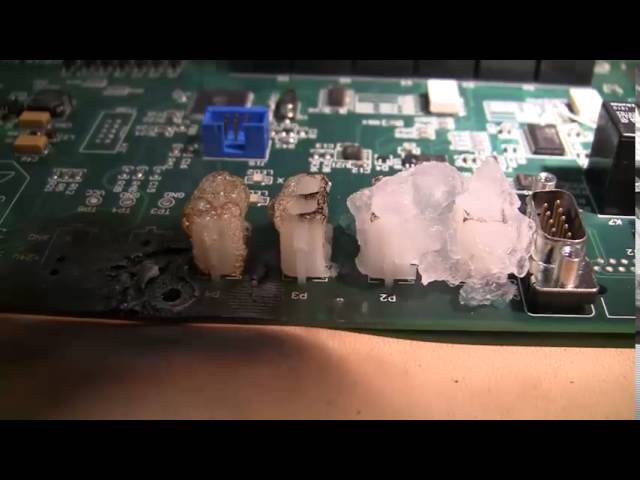
Novel method for protecting electronic components from heat.
.1.jpg)
Technical Library | 2015-08-27 15:32:16.0
Ever since there has been a widespread usage of surface mount parts, the trend of continued shrinkage of devices with ever finer pitches has continued to challenge PCB assemblers for the rework of same. Todays' pitches are commonly 0.5 to 0.4mm with packages of tiny outline sizes, 5 -10mm square, making the rework of such devices a challenge. In addition to the handling and inspection challenges comes the board density. Spacing to neighboring components continues to be compressed so the rework techniques should not damage neighboring components.
Technical Library | 2012-12-17 22:05:22.0
Package on Package (PoP) has become a relatively common component being used in mobile electronics as it allows for saving space in the board layout due to the 3D package layout. To insure device reliability through drop tests and thermal cycling as well as for protecting proprietary programming of the device either one or both interconnect layers are typically underfilled. When underfill is applied to a PoP, or any component for that matter, there is a requirement that the board layout is such that there is room for an underfill reservoir so that the underfill material does not come in contact with surrounding components. The preferred method to dispensing the underfill material is through a jetting process that minimizes the wet out area of the fluid reservoir compared to traditional needle dispensing. To further minimize the wet out area multiple passes are used so that the material required to underfill the component is not dispensed at once requiring a greater wet out area. Dispensing the underfill material in multiple passes is an effective way to reduce the wet out area and decrease the distance that surrounding components can be placed, however, this comes with a process compromise of additional processing time in the underfill dispenser. The purpose of this paper is to provide insight to the inverse relationship that exists between the wet out area of the underfill reservoir and the production time for the underfill process.

Training Courses | | | IPC J-STD-001 Space Specialist (CIS)
The J-STD-001 Space Addendum is an additional optional module for the Certified IPC J-STD-001 CIS (Specialist) program for organizations that are required to meet these additional requirements.
Training Courses | | | PCB Rework and Hand Soldering Courses
The PCB rework and hand soldering courses courses cover techniques of rework and repair of PCBs, BGAs and other electronics assemblies, and teach fundamentals of soldering of electronics assemblies.
Events Calendar | Wed May 12 18:30:00 UTC 2021 - Wed May 12 18:30:00 UTC 2021 | ,
Joint Chapter Meeting: Photonic Soldering
Events Calendar | Wed Jun 12 18:30:00 UTC 2024 - Wed Jun 12 18:30:00 UTC 2024 | Melbourne, Florida USA
Space Coast Event: Maximizing Automation Efficiency: Are You Making the Most of Your Investment?
Career Center | Littleton, Colorado USA | Engineering
If you have experience in Satellite Communications or RF Payload Engineering we have advancement opportunities that may be of interest to you. Available positions are in disciplines such as: Shaped Reflector design and analysis Antenna compo
Career Center | Eden Prairie, Minnesota USA | Production
Solderer ALL SHIFTS Logic PD collaborates with clients to help them launch products that accelerate growth and capture value in the Internet of Things (IoT). Logic PD helps at any stage in the product lifecycle by being the complete product innovat
Career Center | New Delhi, India | Engineering,Research and Development
I have 2 Years experience in SMT,THT and BGA components and 3+ years experience in total. Currently,working in a CMMi LEVEL 5 enviornment. I have been Working on various Panasonic series machines and fuji components. My work profile involves : 1. Si
Career Center | New Delhi, India | Engineering,Research and Development,Technical Support
I have 2 Years experience in SMT,THT and BGA components and 3+ years experience in total. Currently,working in a CMMi LEVEL 5 enviornment. I have been Working on various Panasonic series machines and fuji components. My work profile involves : 1. Si
SMTnet Express, March 12, 2015, Subscribers: 22,490, Members: Companies: 14,252 , Users: 37,867 Miniaturization with Help of Reduced Component to Component Spacing Jonas Sjoberg, Ranilo Aranda, David Geiger, Anwar Mohammed, Murad Kurwa
PCB Libraries, Inc. | https://www.pcblibraries.com/Forum/pdf-print-output-feature_topic760_post2708.html
. Then you insert the component package outline around (or inside the hole pattern) and save to a PKG file format. The hole locations can be on many different grid spacings and various hole sizes and plating options
GPD Global | https://www.gpd-global.com/co_website/pdf/lead-former/CF9-User-Guide-901-1-07.pdf
hole-to-hole spacings. • Controls accuracy and repeatability through the use of a solid gear train, cam, and cam follower indexing system. Most cutting and forming needs are covered with the standard dies we offer. Several of the most common component


