
Industry Directory | Consultant / Service Provider / Media / Publisher / Online Resource / Other
PCB Libraries' "Footprint Expert" suite uses CAD LEAP(tm) Technology to greatly simplify footprint and 3D STEP model creation; it is used by tens of thousands of PCB designers and engineers all over the world.
Industry Directory | Manufacturer
Additive modifies bare PCBs by adding solid copper traces, SMT Pads and deletes even under BGAs. RoHS / non-RoHS bare boards when engineering changes are needed and re-design is not done. Improve quality, thru-put and reliabilty while lowering cost.

The PCB Footprint Expert is a powerful CAD library development tool powered by our own proprietary CAD LEAP Technology (Libraries Enhanced with Automated Preferences). It is packed with very powerful advanced library management features that cuts foo
New Equipment | Fabrication Services
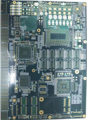
HDI PCB Manufacturer & Assembly – One-stop services from China -HDI (high-density interconnection board) is a compact circuit board designed for small capacity users. Compared with ordinary PCB, the most significant feature of HDI is that the wiri
Electronics Forum | Tue Feb 09 16:53:06 EST 2021 | SMTA-64387083
The size of the pad changes among the two. A solder mask defined pad will always be larger than a copper defined by your mask expansion setting. This will affect paste volume, if your standard paste aperture is designed for copper defined pads you m
Electronics Forum | Wed Apr 04 19:25:58 EDT 2007 | TB
Dear All, anyone has experienced with thin layer of immersion tin (about 5 microns) on copper pads in term of long term reliability for first or second reliability studies. Any input will be greatly appriciated.. Thanks.
Industry News | 2003-06-24 08:14:51.0
R/flex� 3850 laminate is produced in a range of copper and LCP thicknesses, just as the single-clad laminate, and is available in standard panel formats.
Industry News | 2003-06-10 08:16:44.0
The following text describes the application of NWA Quality Analyst to quality control in the assembly of electronic components.
_1.jpg)
Parts & Supplies | Pick and Place/Feeders
FUJI placement machine XP243 suction nozzle copper gasket DBPH0151 Model: FUJI Mounter Specification: PZ34281 Part No.: PZ34281 Name: NXT spring A5054H FUJI seal ABTRG1120 FUJI GL541 dispenser glue package BTPT0961 FUJI belt pulley BTRG0391
_1.jpg)
Parts & Supplies | Pick and Place/Feeders
0808 0808S gland copper gasket 4-000-250-01 4-268-373-02 We sell the following accessories: X-4700-022-1 Wheel Ass'y (8*4 gear) X-2320-959-3 LINER ASSY, MAGNET Feida magnetic copper gasket 4-702-744-02 Lever, Positioning 4-702-751-01 Co
Technical Library | 2008-04-08 17:42:27.0
Concern about the failure of lead-free BGA packages when portable devices such as cell phones are accidentally dropped and a general concern about the resistance of these packages under shock loading has prompted an interest in the impact strength of the soldered BGA connection. This paper reports the results of the measurement of the impact strength of lead-free 0.5±0.01mm diameter BGA spheres on 0.42mm solder mask defined pads on copper/OSP and ENIG substrates using recently developed equipment that can load individual BGA spheres at high strain rates in shear and tension.
Technical Library | 2020-08-27 01:22:45.0
Initially adopted internal specifications for acceptance of printed circuit boards (PCBs) used for wire bonding was that there were no nodules or scratches allowed on the wirebond pads when inspected under 20X magnification. The nodules and scratches were not defined by measurable dimensions and were considered to be unacceptable if there was any sign of a visual blemish on wire-bondable features. Analysis of the yield at a PCB manufacturer monitored monthly for over two years indicated that the target yield could not be achieved, and the main reasons for yield loss were due to nodules and scratches on the wirebonding pads. The PCB manufacturer attempted to eliminate nodules and scratches. First, a light-scrubbing step was added after electroless copper plating to remove any co-deposited fine particles that acted as a seed for nodules at the time of copper plating. Then, the electrolytic copper plating tank was emptied, fully cleaned, and filtered to eliminate the possibility of co-deposited particles in the electroplating process. Both actions greatly reduced the density of the nodules but did not fully eliminate them. Even though there was only one nodule on any wire-bonding pad, the board was still considered a reject. To reduce scratches on wirebonding pads, the PCB manufacturer utilized foam trays after routing the boards so that they did not make direct contact with other boards. This action significantly reduced the scratches on wire-bonding pads, even though some isolated scratches still appeared from time to time, which caused the boards to be rejected. Even with these significant improvements, the target yield remained unachievable. Another approach was then taken to consider if wire bonding could be successfully performed over nodules and scratches and if there was a dimensional threshold where wire bonding could be successful. A gold ball bonding process called either stand-off-stitch bonding (SSB) or ball-stitch-on-ball bonding (BSOB) was used to determine the effects of nodules and scratches on wire bonds. The dimension of nodules, including height, and the size of scratches, including width, were measured before wire bonding. Wire bonding was then performed directly on various sizes of nodules and scratches on the bonding pad, and the evaluation of wire bonds was conducted using wire pull tests before and after reliability testing. Based on the results of the wire-bonding evaluation, the internal specification for nodules and scratches for wirebondable PCBs was modified to allow nodules and scratches with a certain height and a width limitation compared to initially adopted internal specifications of no nodules and no scratches. Such an approach resulted in improved yield at the PCB manufacturer.

The PCB Footprint Expert is a powerful CAD library development tool powered by our own proprietary CAD LEAP Technology (Libraries Enhanced with Automated Preferences). It is packed with very powerful advanced library management features that cuts foo

PCB pad circuit repair using epoxy. Using multiple angles including overhead and from both right and left angles the BEST instructor staff demonstrates plainly how to repair a PCB pad using the epoxy method. This method is per IPC 7721 4.4.1. http://
Training Courses | | | Other Courses
Other courses related to electronics manufacturing and assembly
Training Courses | | | PCB Design Courses
The PCB design courses teach students the process, techniques and tools needed to design layout of printed circuit boards.
Events Calendar | Wed Apr 20 00:00:00 EDT 2022 - Wed Apr 20 00:00:00 EDT 2022 | ,
Virtual Course: Selection Criteria of Surface Finish for Next Generation PCB Technologies
Events Calendar | Mon Apr 23 00:00:00 EDT 2018 - Thu Apr 26 00:00:00 EDT 2018 | Shanghai, China
SMTA China East Conference 2018
Career Center | Wellsboro, Pennsylvania USA | Engineering
SMT PROCESS ENGINEER: (Wellsboro, PA) - Designs, defines and plans the manufacturing process. Specifies and directs installation of new processes. Plans equipment build schedules and monitors vendor progress. Defines and recommends equipment, methods
Career Center | Bangalore, India | Engineering,Maintenance,Production,Technical Support
SMT Stencil designing & Knowledge of full SMT process software known CAD/CAM -circuit CAM Pro 7.3,GC Power station, GCCAM Edit,Auto CAD, Fault finding of Electronic Boards & Servicing electronic machines.
Career Center | Stoneham, Massachusetts | Engineering,Production,Research and Development,Technical Support
Warren P. Pumyea 8 Beacon Street Stoneham, Massachusetts 02180 Cell #: 978-821-7335 * E-mail: warren@pumyea.com http://www.pumyea.com/Process_Manufacturing_Engineer.doc Objective: Seeking a position as an engineer or related discipline whic
| https://www.eptac.com/faqs/ask-helena-leo/ask/addressing-missing-pcb-pads-from-soldering-rework
: This is a difficult topic to answer as it has to be defined between the manufacturer and the supplier or customer. As stated, if the pads were removed during the rework process, the board was damaged and this will have to be documented and dis-positioned
Imagineering, Inc. | https://www.pcbnet.com/capabilities/fabrication/tolerances/
. They provide enough variation for us to manufacture your board – and for it to work properly in your application. Copper to Edge of Printed Circuit Board Minimum of 0.007″ (outer layers) and 0.015″ for inner layers (0.020
winsouce.jpg)


