Industry Directory | Distributor / Manufacturer
Top 20 High-Quality PCB Fabrication and one-stop Turnkey PCB Assembly Facilities worldwide. Served national engineers for over 15 years, becoming a household name in providing full-feature multilayer PCBs engineers can trust.
New Equipment | Test Equipment
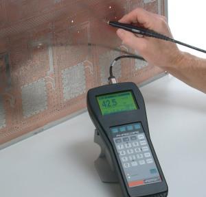
The hand-held PHASCOPE® PMP10 is ideally suited for quality control in the electroplating and printed circuit board (PCB) industries. Because the instrument employs the phase-sensitive eddy current method (ISO 21 968), it allows the measurement of me
New Equipment | Test Equipment
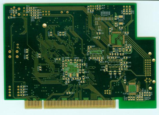
Printed Circuit Boards(PCBs) are used to electrically connect electronic components using conductive pathways, traces, etched from copper sheets laminated onto a non-conductive substrate. Our manufacturing processes utilise the latest techniques an
Electronics Forum | Mon Nov 15 21:35:50 EST 1999 | Dave F
Bob Bob: Fortunately, you found this before you built-up a lot of product. Some thoughs and other drivel: 1 Use IPC-TM-650, Method 2.4.8 for copper peel with a Instron machine. Typical pad peel strength requirement for FR-4, 2 oz. copper is: 6 l
Electronics Forum | Thu Mar 04 17:10:19 EST 1999 | Earl Moon
| Our vendor proposed to supply us with shields made out of Cold Rolled Steel (CRS) electroplated with Sn (50 - 150 minches). Should I be concerned with solderability or are there a better alternatives to tin finish? | No matter the base metal, elec
Industry News | 2011-10-03 15:37:21.0
The SMTA announced a session on Challenges and Solutions for PCB Technology which will take place on Tuesday, October 18 during their annual conference, SMTA International
Industry News | 2018-10-18 11:08:03.0
Different Techniques for Plating
Technical Library | 2021-05-26 00:53:26.0
This paper describes a copper electroplating enabling technology for filling microvias. Driven by the need for faster, smaller and higher performance communication and electronic devices, build-up technology incorporating microvias has emerged as a viable multilayer printed circuit manufacturing technology. Increased wiring density, reduced line widths, smaller through-holes and microvias are all attributes of these High Density Interconnect (HDI) packages. Filling the microvias with conductive material allows the use of stacked vias and via in pad designs thereby facilitating additional packaging density. Other potential design attributes include thermal management enhancement and benefits for high frequency circuitry. Electrodeposited copper can be utilized for filling microvias and provides potential advantages over alternative via plugging techniques. The features, development, scale up and results of direct current (DC) and periodic pulse reverse (PPR) acid copper via filling processes, including chemistry and equipment, are described.
Technical Library | 2017-11-22 12:38:51.0
The use of copper foils laminated to polyimide (PI) as flexible printed circuit board precursor is a standard practice in the PCB industry. We have previously described[1] an approach to very thin copper laminates of coating uniform layers of nano copper inks and converting them into conductive foils via photonic sintering with a multibulb conveyor system, which is consistent with roll-to-roll manufacturing. The copper thickness of these foils can be augmented by electroplating. Very thin copper layers enable etching fine lines in the flexible circuit. These films must adhere tenaciously to the polyimide substrate.In this paper, we investigate the factors which improve and inhibit adhesion. It was found that the ink composition, photonic sintering conditions, substrate pretreatment, and the inclusion of layers (metal and organic) intermediate between the copper and the polyimide are important.
With the development of miniaturization of assembly components, the layout area and pattern design area of PCBs have also been continuously reduced, and PCB manufacturers are constantly updating the production process to conform to the development tr
Events Calendar | Fri Apr 16 00:00:00 EDT 2021 - Fri Apr 16 00:00:00 EDT 2021 | ,
Auburn University Student Chapter Event: Get Hired in Electronics Industry
Events Calendar | Tue Dec 04 00:00:00 EST 2018 - Tue Dec 04 00:00:00 EST 2018 | ,
Qualification and Reliability of Microvias
SMTnet Express, May 27, 2021, Subscribers: 27,090, Companies: 11,365, Users: 26,673 Filling of Microvias and Through Holes by Electrolytic Copper Plating - Current Status and Future Outlook The electronics industry is further
SMTnet Express, May 12, 2022, Subscribers: 25,588, Companies: 11,569, Users: 27,213 Electronics Manufacturing Technical Articles Filling of Microvias and Through Holes by Electrolytic Copper Plating –Current Status and Future
Imagineering, Inc. | https://www.pcbnet.com/blog/what-is-the-pcb-fabrication-process/
. Once removed, a thin coating of copper is deposited on all exposed parts of a panel, creating a metallic base for the electroplating process
Surface Mount Technology Association (SMTA) | https://www.smta.org/panpac/Pan-Pacific-2020-Program.pdf?v=20060405647
., Auburn University Copper Electrodeposition by Hydrogen Evolution Assisted (HEA) Electroplating for Wearable Electronics Sabrina Rosa-Ortiz, University of South Florida Glass Panel Packaging as the Most Leading-Edge Packaging: R


