
Industry Directory | Consultant / Service Provider / Manufacturer / Other
ScanCAD is an industry leader in inspection, measurement, process control and reverse engineering. Our solutions support OEM's, manufacturers, stencil fabricators, repair depots, and others in optimizing quality and yield.

Industry Directory | Consultant / Service Provider / Media / Publisher / Online Resource / Other
PCB Libraries' "Footprint Expert" suite uses CAD LEAP(tm) Technology to greatly simplify footprint and 3D STEP model creation; it is used by tens of thousands of PCB designers and engineers all over the world.
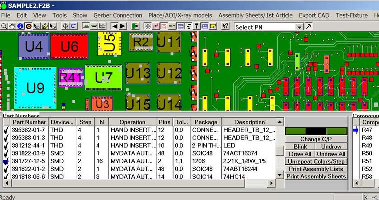
If you have only Gerber data files to work with then ProntoGERBER-CONNECTION can help you! ProntoGERBER-CONNECTION imports raw Gerber data and allows the user to add intelligent information to the shapes on the display and create process assembly

The PCB Footprint Expert is a powerful CAD library development tool powered by our own proprietary CAD LEAP Technology (Libraries Enhanced with Automated Preferences). It is packed with very powerful advanced library management features that cuts foo
Electronics Forum | Fri Nov 27 00:36:02 EST 2015 | slouis2014
I just encountered a BGA design were in, underneath the BGA is a silkscreen that covered the entire bottom of the component except for the copper pads. Can you give any information and advice for this type of design.
Electronics Forum | Fri Dec 04 05:47:57 EST 2015 | rushpcbuk
In PCB design, a BGA (Ball Grid Array) package typically determines the number of layers that a Printed Circuit Board should have. However, the 4-layer board with a BGA package is commonly used than a 2-layer than an 8-layer PCB. On the other hand, t
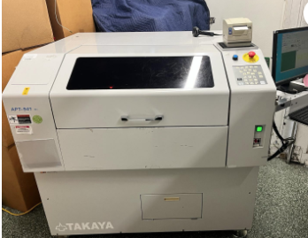
Used SMT Equipment | In-Circuit Testers
Description Make: Takaya Model: APT-9411CE Year: 2010 Type: Flying Probe Details: Takaya APT 9411 CE Flying Probe The APT-9411CE is designed for users who are looking for a precise and reliable test system with an easy to use softwar
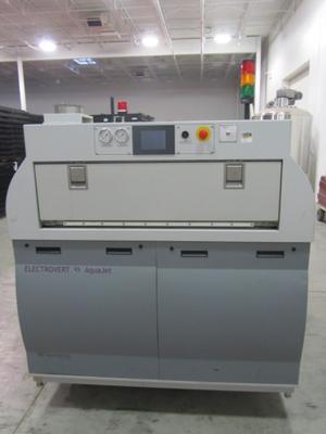
Used SMT Equipment | Board Cleaners
Speedline Technologies AquaJet Stencil Batch Cleaner and Resys ClosedLoop System For Sale The wash needs a control board. (Part Description: BL1700 CNTRL 16IN 16OUT) The Part Number to Purchase this board is 20-101-0214. Estimated cost is $349. We h
Industry News | 2003-06-24 08:14:51.0
R/flex� 3850 laminate is produced in a range of copper and LCP thicknesses, just as the single-clad laminate, and is available in standard panel formats.
Industry News | 2003-06-17 08:07:40.0
The Radiall SMT coupler range now includes the new 14.2 x 5.1mm mini type.
_1.jpg)
Parts & Supplies | Pick and Place/Feeders
FUJI placement machine XP243 suction nozzle copper gasket DBPH0151 Model: FUJI Mounter Specification: PZ34281 Part No.: PZ34281 Name: NXT spring A5054H FUJI seal ABTRG1120 FUJI GL541 dispenser glue package BTPT0961 FUJI belt pulley BTRG0391
_1.jpg)
Parts & Supplies | Pick and Place/Feeders
0808 0808S gland copper gasket 4-000-250-01 4-268-373-02 We sell the following accessories: X-4700-022-1 Wheel Ass'y (8*4 gear) X-2320-959-3 LINER ASSY, MAGNET Feida magnetic copper gasket 4-702-744-02 Lever, Positioning 4-702-751-01 Co
Technical Library | 2019-05-29 01:47:22.0
1.Vias near SMD pads: Solder can flow into the via after melted. As a result cold joint will appear in the end. Check the picture below. 2.Vias on SMD pads: Solder can flow into the via more easier after melted. Check the picture below. 3.Via opening without soldermask covered. When workers solder TH parts by hand, soldering iron can touch vias sometime, then tiny amounts molten solder will stay on vias. This can lead to electrical short easily. We recommend you make all vias tenting (covered by solder mask) if it is possible.
PCBNPI-Professional PCB Fab/PCB Assembly Service Provider From China
Technical Library | 1999-05-07 08:45:39.0
Fine pitch SMT devices, although certainly not new, present more of an assembly processing challenge than 50 mil pitch devices. In fact it seems that the finer the pitch the more difficult or narrower the process window becomes. Besides the pitch of the leads being less on fine pitch devices narrower pad width on the board is typical. With fine pitch designs the board fabrication process is also stressed in that the strip of mask between the pads is designed narrower, the alignment of the mask to copper becomes more critical

Nano-copper sintering in formic acid vapor.
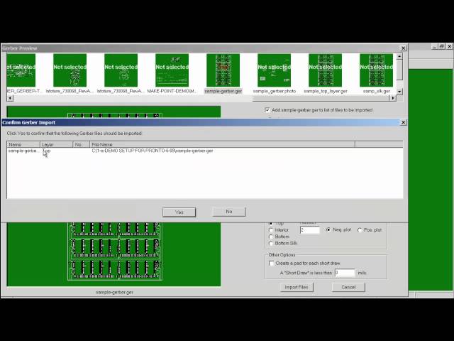
ProntoGERBER-CONNECTION software is used by electronic manufacturer & imports raw Gerber data & allows the user to add intelligent information to the shapes on the display and creates real reference designators, theta rotation, part numbers, X/Y comp
Training Courses | | | IPC-600 Specialist (CIS)
The Certified IPC-600 Specialist (CIS) training targets quality assurance and acceptance of bare printed circuit boards.
Training Courses | | | PCB Rework and Hand Soldering Courses
The PCB rework and hand soldering courses courses cover techniques of rework and repair of PCBs, BGAs and other electronics assemblies, and teach fundamentals of soldering of electronics assemblies.
Events Calendar | Wed Apr 20 00:00:00 EDT 2022 - Wed Apr 20 00:00:00 EDT 2022 | ,
Virtual Course: Selection Criteria of Surface Finish for Next Generation PCB Technologies
Events Calendar | Mon Apr 23 00:00:00 EDT 2018 - Thu Apr 26 00:00:00 EDT 2018 | Shanghai, China
SMTA China East Conference 2018
Career Center | Sherman, Texas USA | Engineering,Production,Research and Development,Technical Support
SMT Packaging Engineer: Location: Texas - Sherman , TX Group: HVAL Degree Requirements: BS ME/ChemE/Materials The person in this position will have the ability to make very significant financial contributions to TI because this is a very critic
Career Center | Lincoln, Nebraska USA | Engineering
Brief Description of Job Duties: Provide new program engineering support with emphasis on technical SMT process development. Key activities would include recommendations and implementation of components, SMT pad design, solder methods, testing and r
Career Center | Bangalore, India | Engineering,Maintenance,Production,Technical Support
SMT Stencil designing & Knowledge of full SMT process software known CAD/CAM -circuit CAM Pro 7.3,GC Power station, GCCAM Edit,Auto CAD, Fault finding of Electronic Boards & Servicing electronic machines.
Career Center | Newport Beach, California USA | Engineering,Management,Production
KEVIN RAGER P.O.BOX 7878, NEWPORT BEACH, 949 922 8997, KEVIN.RAGER@EDA-INC.US OBJECTIVE I am trying to find a consistent work flow that provides mentally challenging yet stimulating experiences in design and prototype development. EXPERIENCE 1997
Pad Cratering - The Invisible Threat to the Electronics Industry SMTnet Express September 6, 2012, Subscribers: 25455, Members: Companies: 8972, Users: 33613 Pad Cratering - The Invisible Threat to the Electronics Industry First published
PCB Libraries, Inc. | https://www.pcblibraries.com/forum/design-smt-pad-for-magnet-wire_topic1206.html
Design SMT pad for magnet wire - PCB Libraries Forum Forum Home > PCB Footprint Expert > Questions & Answers New Posts FAQ Search Events Register Login Design SMT pad for magnet wire
Imagineering, Inc. | https://www.pcbnet.com/blog/understanding-the-pcb-fabrication-process-from-design-to-delivery/
. Once the manufacturer prints the design onto a piece of laminate material, it applies a layer of copper foil or coating. This process bonds the copper to the laminate, creating the PCB’s structure


