Industry Directory | Manufacturer
Additive modifies bare PCBs by adding solid copper traces, SMT Pads and deletes even under BGAs. RoHS / non-RoHS bare boards when engineering changes are needed and re-design is not done. Improve quality, thru-put and reliabilty while lowering cost.
Industry Directory | Manufacturer
One-Stop Solution for PCB & Prototype Assembly Expanded PCB manufacturing capabilities to support advanced designs with demanding requirements including laser-drilled microvias, cavity boards, heavy copper up to 20 oz., via-in-pad

CAMMaster CAMMaster is the premier product for the most demanding jobs, with scripting features to automate your routine jobs and improve accuracy and yields to get the work done faster. CAMMaster features: Advanced DFM checks Netlist ex
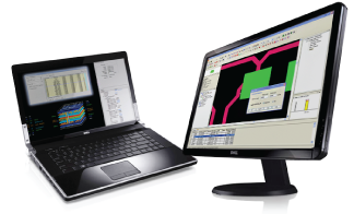
Design For Manufacturability And Yield Enhancement. The Design for Manufacturability (DFM) engine searches for fabrication issues and discovers areas where yields may be increased. GraphiCode's Contour Technology produces fast and accurate results f
Electronics Forum | Mon Nov 15 21:35:50 EST 1999 | Dave F
Bob Bob: Fortunately, you found this before you built-up a lot of product. Some thoughs and other drivel: 1 Use IPC-TM-650, Method 2.4.8 for copper peel with a Instron machine. Typical pad peel strength requirement for FR-4, 2 oz. copper is: 6 l
Electronics Forum | Thu Nov 25 20:28:43 EST 1999 | cklau
hello, One way to prevent copper land delamination is to applied Anchoring spurs also referred to as "tie-down tabs" or "rabbit ears".These are a metal projection around a land.This features is fully captured by the cover lay (cover coat) that is n
Industry News | 2018-08-16 19:58:50.0
The SMTA Capital Chapter is holding its upcoming Capital Expo and Tech Forum at Johns Hopkins University / Applied Physics Lab, Kossiakoff Center, 11100 Johns Hopkins Road, Laurel, MD 20723, on Thursday, August 23rd.
Industry News | 2015-11-25 16:58:05.0
On behalf of the SMTA International Technical Committee, we invite you to submit a 300 word abstract of your research for the 2016 SMTA International 2016 technical conference in Rosemont, Illinois. Papers should describe significant results from experiments, emphasize new techniques, and contain technical, economic or appropriate test data. We are looking for papers on a variety of topics related to electronics manufacturing including advanced packaging/components, assembly, business/supply chain, emerging technologies, harsh environment applications, PCB technology, and process control. Materials must be original, unpublished and non-commercial in nature.
_1.jpg)
Parts & Supplies | Pick and Place/Feeders
FUJI placement machine XP243 suction nozzle copper gasket DBPH0151 Model: FUJI Mounter Specification: PZ34281 Part No.: PZ34281 Name: NXT spring A5054H FUJI seal ABTRG1120 FUJI GL541 dispenser glue package BTPT0961 FUJI belt pulley BTRG0391
_1.jpg)
Parts & Supplies | Pick and Place/Feeders
0808 0808S gland copper gasket 4-000-250-01 4-268-373-02 We sell the following accessories: X-4700-022-1 Wheel Ass'y (8*4 gear) X-2320-959-3 LINER ASSY, MAGNET Feida magnetic copper gasket 4-702-744-02 Lever, Positioning 4-702-751-01 Co
Technical Library | 2012-09-06 18:19:37.0
First published in the 2012 IPC APEX EXPO technical conference proceedings. Pad Cratering opens circuits. This occurs when the resin crack (fracture) migrates through a copper trace or via. This happens at assembly, in service or during handling. When com
Technical Library | 2016-10-20 18:13:34.0
Pad cratering failure has emerged due to the transition from traditional SnPb to SnAgCu alloys in soldering of printed circuit assemblies. Pb-free-compatible laminate materials in the printed circuit board tend to fracture under ball grid array pads when subjected to high strain mechanical loads. In this study, two Pb-free-compatible laminates were tested, plus one dicycure non-Pb-free-compatible as control. One set of these samples were as-received and another was subjected to five reflows. It is assumed that mechanical properties of different materials have an influence on the susceptibility of laminates to fracture. However, the pad cratering phenomenon occurs at the layer of resin between the exterior copper and the first glass in the weave. Bulk mechanical properties have not been a good indicator of pad crater susceptibility. In this study, mechanical characterization of hardness and Young’s modulus was carried out in the critical area where pad cratering occurs using nano-indentation at the surface and in a cross-section. The measurements show higher modulus and hardness in the Pb-free compatible laminates than in the dicy-cured laminate. Few changes are seen after reflow – which is known to have an effect -- indicating that these properties do not provide a complete prediction. Measurements of the copper pad showed significant material property changes after reflow.

The PCB Footprint Expert is a powerful CAD library development tool powered by our own proprietary CAD LEAP Technology (Libraries Enhanced with Automated Preferences). It is packed with very powerful advanced library management features that cuts foo

PCB pad circuit repair using epoxy. Using multiple angles including overhead and from both right and left angles the BEST instructor staff demonstrates plainly how to repair a PCB pad using the epoxy method. This method is per IPC 7721 4.4.1. http://
Events Calendar | Wed Apr 20 00:00:00 EDT 2022 - Wed Apr 20 00:00:00 EDT 2022 | ,
Virtual Course: Selection Criteria of Surface Finish for Next Generation PCB Technologies
Events Calendar | Mon Apr 23 00:00:00 EDT 2018 - Thu Apr 26 00:00:00 EDT 2018 | Shanghai, China
SMTA China East Conference 2018
Career Center | Bangalore, India | Engineering,Maintenance,Production,Technical Support
SMT Stencil designing & Knowledge of full SMT process software known CAD/CAM -circuit CAM Pro 7.3,GC Power station, GCCAM Edit,Auto CAD, Fault finding of Electronic Boards & Servicing electronic machines.
Imagineering, Inc. | https://www.pcbnet.com/capabilities/fabrication/tolerances/
. They provide enough variation for us to manufacture your board – and for it to work properly in your application. Copper to Edge of Printed Circuit Board Minimum of 0.007″ (outer layers) and 0.015″ for inner layers (0.020


