Industry Directory | Manufacturer
CVInc services advanced packaging. Placing solder bumps on single die, partial wafers, and complete wafers...we also offer RDL (redistribution) services in 5-7 working days. Our custom preforms are as small as 50um geometries.
Industry Directory | Manufacturer
Isola a global material sciences company focused on designing, developing, manufacturing and marketing copper-clad laminates and dielectric prepregs used to fabricate advanced multilayer PCBs.
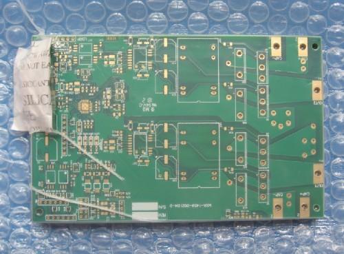
1). 6 oz (210μm) on BOT side. 2). 139.99*110.85mm=1 pcb 3). Base material: FR-4 4). 4 Layer, 1.6mm thick 5). Green solder mask/ white legend 6). Immersion gold. 7). Stack-up ---------- OVERLAY (TOP) ---------- SOLDER MASK (TOP)
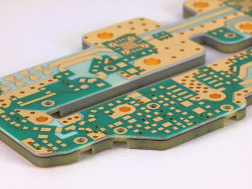
Consisting of multiple laminates and differing dielectric constants, this multilayer (displayed right) is a mixed-dielectric printed circuit board which was manufactured for the Aerospace Industry. Multilayer Mixed Dielectric PCB Specifications:
Electronics Forum | Mon Nov 07 12:25:32 EST 2005 | Rob
Hi CW, Larger chip caps can be susceptable to cracking, but mainly this is due to handling - flexing of boards is the main culprit (the part being mechanically joined at both ends to the board). PCB's usually flex easiest along one axis, and larger
Electronics Forum | Wed Jun 21 08:31:36 EDT 2006 | don dawson
Depending on the material, the etching can damage the dielectric. This can be manufactured but is difficult and expensive. Copper plating and other processes that require agitation are almost impossible.
Industry News | 2003-06-24 08:14:51.0
R/flex� 3850 laminate is produced in a range of copper and LCP thicknesses, just as the single-clad laminate, and is available in standard panel formats.
Parts & Supplies | Circuit Board Assembly Products
1) Woven Glass-Reinforced PTFE 2) Single side/Double sided, 3) Dielectric constant Er:= 2.55, 2.65, 2.75, 2.90, 3.0, 3.5 4) Copper weight: 0.5 - 3 oz 5) PCB thickness: 0.17-3.0mm 6) Track/space: per drawing 7) Finish: Copper finish.
Technical Library | 2012-02-16 16:53:16.0
Channel simulations are only as accurate as the models used to develop them. While we have seen much effort placed on printed circuit board (PCB) materials (copper finish, dielectric moisture absorption), other elements within the channel have been largel
Technical Library | 2015-04-30 20:17:03.0
Higher-speed signal transmission is increasingly required on a printed circuit board to handle massive data in electronic systems. So, signal transmission loss of copper wiring on a printed circuit board has been studied. First, total signal loss was divided into dielectric loss and conductor loss quantitatively based on electromagnetic theory. In particular, the scattering loss due to surface roughness of copper foil has been examined in detail. And the usefulness of the copper foil with low surface roughness has been demonstrated.

This video describes the IPC A-600 training and certification program. The IPC A-600 specification is a set of acceptability specifications for printed circuit boards. These standards determine the acceptance and reject criteria for printed wiring bo
This video describes the IPC A-600 training and certification program. The IPC A-600 specification is a set of acceptability specifications for printed circuit boards. These standards determine the acceptance and reject criteria for printed wiring bo
Training Courses | | | IPC-600 Specialist (CIS)
The Certified IPC-600 Specialist (CIS) training targets quality assurance and acceptance of bare printed circuit boards.
Training Courses | | | IPC-600 Specialist (CIS)
The Certified IPC-600 Specialist (CIS) training targets quality assurance and acceptance of bare printed circuit boards.
Career Center | Erode, Tamilnadu India | Engineering
Professional Summary 3+ years of experience in the PCB CAM engineering Exposure to FRONTLINE GENESIS 2000 Having exposure in UCAM Exposure to Create, Array & Panelize it for manufacturability Experienced in Creating impedance cou
SMTnet Express, April 30, 2015, Subscribers: 22,686, Members: Companies: 14,334 , Users: 38,119 Signal Transmission Loss due to Copper Surface Roughness in High-Frequency Region Elaine Liew; Mitsui Copper Foil Malaysia, Shah Alam Malaysia, Taka
SMTnet Express, February 14, 2019, Subscribers: 31,675, Companies: 10,706, Users: 25,728 Influence of Copper Conductor Surface Treatment for High Frequency PCB on Electrical Properties and Reliability Credits: MEC Company Ltd. Development
PCB Libraries, Inc. | https://www.pcblibraries.com/forum/hdi-material-selection_topic3243.html
. Is there an equivalent range of overall thickness of the board that is common in HDI boards. And are there standard material configurations of copper and dielectric, of given thicknesses, to achieve these overall thicknesses
ASYMTEK Products | Nordson Electronics Solutions | https://www.nordson.com/en/divisions/efd/resource-center/thermal-compound-glossary
) has the minimum thermal resistance. Thermal resistance will not change at thickness less than this value. C D Dielectric Constant A measure of a substance's ability to insulate charges from each other


winsouce.jpg)