Industry Directory | Manufacturer
Additive modifies bare PCBs by adding solid copper traces, SMT Pads and deletes even under BGAs. RoHS / non-RoHS bare boards when engineering changes are needed and re-design is not done. Improve quality, thru-put and reliabilty while lowering cost.
Precision casting foundary who has achieved a reputation as an aggressive leader in the production of investment casting, permanent mold casting and rapid prototype casting.
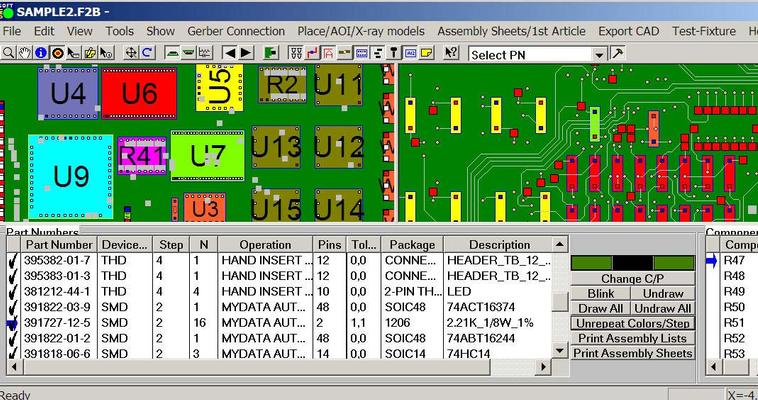
If you have only Gerber data files to work with then ProntoGERBER-CONNECTION can help you! ProntoGERBER-CONNECTION imports raw Gerber data and allows the user to add intelligent information to the shapes on the display and create process assembly

The PCB Footprint Expert is a powerful CAD library development tool powered by our own proprietary CAD LEAP Technology (Libraries Enhanced with Automated Preferences). It is packed with very powerful advanced library management features that cuts foo
Electronics Forum | Thu Apr 15 11:15:30 EDT 2004 | patrickbruneel
Pure (red) copper oxide is green, its not a residue its just oxidation. In your case water and heat will accelerate the oxidation process of unplated or unprotected pure copper. The best way to avoid this from happening is use a socket with tin or n
Electronics Forum | Thu Apr 15 08:23:47 EDT 2004 | prod
hi, Having put a copper socket trough a wave soldering machine, and then through a DI wash, the boards have been dried and after a few days a green residue has been noticed on the copper. any suggestions? not drying properly maybe? or could it be th
Industry News | 2011-08-18 21:24:08.0
For an industry that is constantly advancing, the technical conference at IPC Midwest Conference & Exhibition on September 21–22, in Schaumburg, Ill., will feature five sessions offering the latest research, methodologies and insights from industry experts to address critical challenges of manufacturing defect-free, quality electronics.
Industry News | 2011-08-18 21:23:09.0
For an industry that is constantly advancing, the technical conference at IPC Midwest Conference & Exhibition on September 21–22, in Schaumburg, Ill., will feature five sessions offering the latest research, methodologies and insights from industry experts to address critical challenges of manufacturing defect-free, quality electronics.
Parts & Supplies | Circuit Board Assembly Products
Specifications 1.One-stop OEM pcb assembly service. 2.ROHS, SGS, UL certificated 3.Reasonable price 4.High Quality 5.Fast Delivery PCB Assembly&PCBA Service 1. Experienced components sourcing team specially for scarce parts 2.1 to 12 layers m
Parts & Supplies | Circuit Board Assembly Products
Specifications 1.One-stop OEM pcb assembly service. 2.ROHS, SGS, UL certificated 3.Reasonable price 4.High Quality 5.Fast Delivery PCB Assembly&PCBA Service 1. Experienced components sourcing team specially for scarce parts 2.1 to 12 layers m
Technical Library | 2016-09-08 16:27:49.0
In this investigation a test matrix was completed utilizing 900 electrodes (small circuit board with parallel copper traces on FR-4 with LPI soldermask at 6, 10 and 50 mil spacing): 12 ionic contaminants were applied in five concentrations to three different spaced electrodes with five replicas each (three different bare copper trace spacing / five replications of each with five levels of ionic concentration). The investigation was to assess the electrical response under controlled heat and humidity conditions of the known applied contamination to electrodes, using the IPC SIR (surface insulation resistance) J-STD 001 limits and determine at what level of contamination and spacing the ionic / organic residue has a failing effect on SIR.
Technical Library | 2020-09-02 22:02:13.0
With the adoption of Wafer Level Packages (WLP) in the latest generation mobile handsets, the Printed Circuit Board (PCB) industry has also seen the initial steps of High Density Interconnect (HDI) products migrating away from the current subtractive processes towards a more technically adept technique, based on an advanced modified Semi Additive Process (amSAP). This pattern plate process enables line and space features in the region of 20um to be produced, in combination with fully filled, laser formed microvias. However, in order to achieve these process demands, a step change in the performance of the chemical processes used for metallization of the microvia is essential. In the electroless Copper process, the critical activator step often risks cross contamination by the preceding chemistries. Such events can lead to uncontrolled buildup of Palladium rich residues on the panel surface, which can subsequently inhibit etching and lead to short circuits between the final traces. In addition, with more demands being placed on the microvia, the need for a high uniformity Copper layer has become paramount, unfortunately, as microvia shape is often far from ideal, the deposition or "throw" characteristics of the Copper bath itself are also of critical importance. This "high throwing power" is influential elsewhere in the amSAP technique, as it leads to a thinner surface Copper layer, which aids the etching process and enables the ultra-fine features being demanded by today's high end PCB applications. This paper discusses the performance of an electroless Copper plating process that has been developed to satisfy the needs of challenging amSAP applications. Through the use of a radical predip chemistry, the formation, build up and deposition of uncontrolled Pd residues arising from activator contamination has been virtually eradicated. With the adoption of a high throwing power Copper bath, sub 30um features are enabled and microvia coverage is shown to be greatly improved, even in complex via shapes which would otherwise suffer from uneven coverage and risk premature failure in service. Through a mixture of development and production data, this paper aims to highlight the benefits and robust performance of the new electroless Copper process for amSAP applications
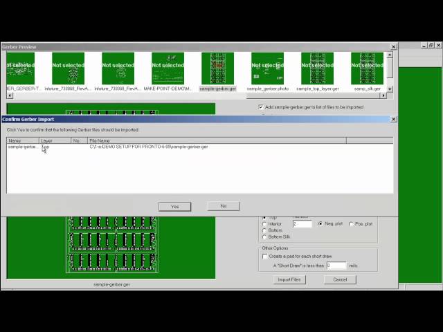
ProntoGERBER-CONNECTION software is used by electronic manufacturer & imports raw Gerber data & allows the user to add intelligent information to the shapes on the display and creates real reference designators, theta rotation, part numbers, X/Y comp

The PCB Footprint Expert is a powerful CAD library development tool powered by our own proprietary CAD LEAP Technology (Libraries Enhanced with Automated Preferences). It is packed with very powerful advanced library management features that cuts foo
Training Courses | | | Other Courses
Other courses related to electronics manufacturing and assembly
Training Courses | | | IPC-600 Specialist (CIS)
The Certified IPC-600 Specialist (CIS) training targets quality assurance and acceptance of bare printed circuit boards.
Events Calendar | Wed Mar 18 00:00:00 EDT 2020 - Wed Mar 18 00:00:00 EDT 2020 | College Park, Maryland USA
CALCE Reliability Science Symposium - Spring 2020
Career Center | Shen Zhen, China | Management,Sales/Marketing
Working in GLORYPCB for 10 years.knowing electronic supply chain very well. especially for PCB PCBA assembly and other Electronic Manufacturing Service.Glorypcb is a professional electronic manufacturer located in Shenzhen with three facilities.offe
Career Center | Erode, Tamilnadu India | Engineering
Professional Summary 3+ years of experience in the PCB CAM engineering Exposure to FRONTLINE GENESIS 2000 Having exposure in UCAM Exposure to Create, Array & Panelize it for manufacturability Experienced in Creating impedance cou
SMTnet Express, Septemeber 8, 2016, Subscribers: 26,370, Companies: 14,943, Users: 41,052 How Clean is Clean Enough – At What Level Does Each of The Individual Contaminates Cause Leakage and Corrosion Failures in SIR? Terry Munson, Paco Solis
Imagineering, Inc. | https://www.pcbnet.com/capabilities/fabrication/tolerances/
. Copper Trace Width/Spacing Copper spacing is the minimum air gap between any two adjacent copper features. Trace width is the minimum width of a copper feature, usually traces
PCB Libraries, Inc. | https://www.pcblibraries.com/forum/RSS_via-naming-convention_topic2038.xml
. If the anti-pad diameter should not be larger than the pad annular ring + trace space. You do not want to run high speed signal traces over a plane anti-pad


