New Equipment | Assembly Services
http://www.flason-smt.com/product/China-second-hand-LED-Assembly-Line-SMT-Assembly-Line-PCBA-Line.html China second hand LED Assembly Line/ SMT Assembly Line/ PCBA Line Name: SMT assembly line Usage: PCB production Type: Semi auto Production t

New Equipment | Assembly Services
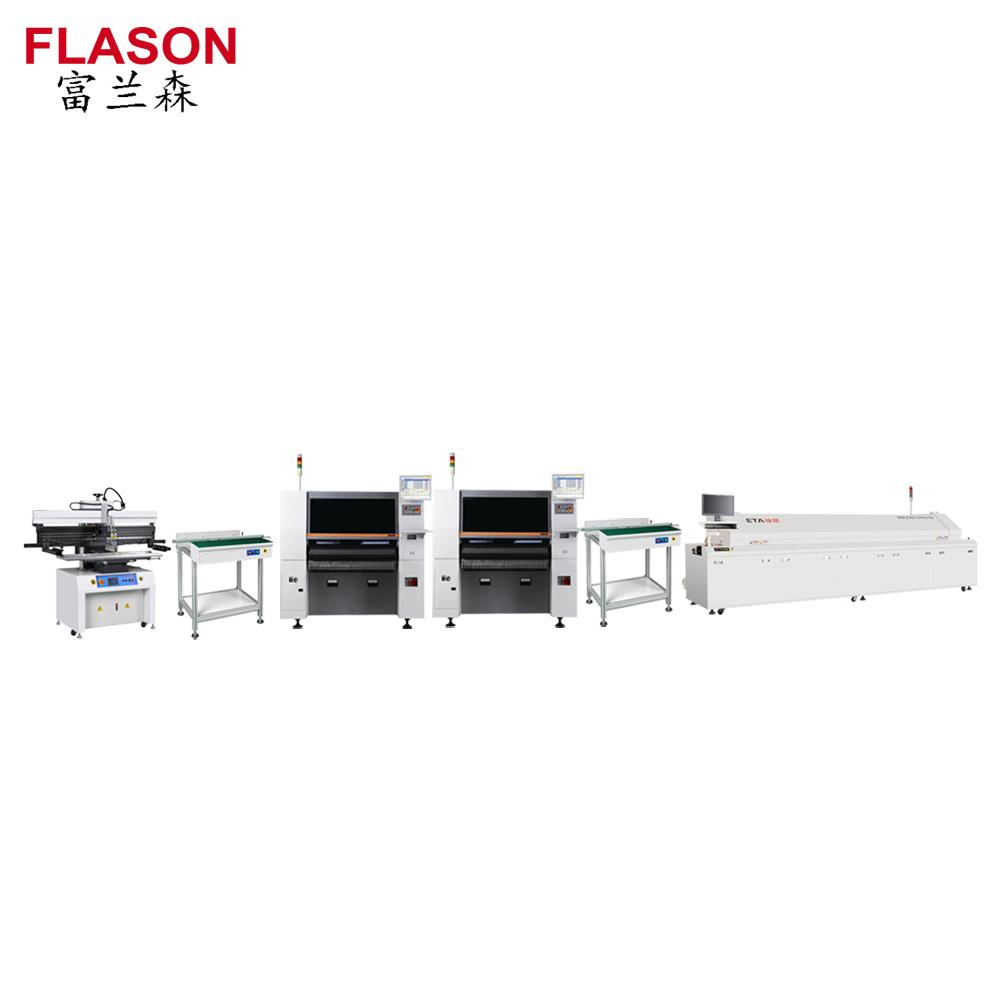
http://www.flason-smt.com/product/LED-Assembly-Line-SMT-Assembly-Line-PCBA-Line-printer-mounter-reflow-oven.html LED Assembly Line/ SMT Assembly Line/ PCBA Line (printer+mounter+reflow oven) Name: SMT assembly line Usage: PCB production Type: S
Industry News | 2026-02-16 15:29:38.0
The SMTA Capital Chapter is pleased to announce an upcoming technical webinar focused on an increasingly critical reliability risk in modern electronics manufacturing: component failure resulting from overexposure to ionizing radiation during manual X-ray solder joint inspection.
Industry News | 2022-10-13 07:44:15.0
I.C.T SMT Vacuum Reflow Oven Machine helps you to solve the problem of High Solder Voids Rates
Technical Library | 2012-12-14 14:28:20.0
This paper examines the potential failure mechanisms that can damage modern lowvoltage CMOS devices and their relationship to electrical testing. Failure mechanisms such as electrostatic discharge (ESD), CMOS latch-up, and transistor gate oxide degradation can occur as a result of electrical over-voltage stress (EOS). In this paper, EOS due to electrical testing is examined and an experiment is conducted using pulsed voltage waveforms corresponding to conditions encountered during in-circuit electrical testing. Experimental results indicate a correlation between amplitude and duration of the pulse waveform and device degradation due to one or more of the failure mechanisms.
Technical Library | 2016-05-19 16:03:37.0
As consumers become more reliant on their handheld electronic devices and take them into new environments, devices are increasingly exposed to situations that can cause failure. In response, the electronics industry is making these devices more resistant to environmental exposures. Printed circuit board assemblies, handheld devices and wearables can benefit from a protective conformal coating to minimize device failures by providing a barrier to environmental exposure and contamination. Traditional conformal coatings can be applied very thick and often require thermal or UV curing steps that add extra cost and processing time compared to alternative technologies. These coatings, due to their thickness, commonly require time and effort to mask connectors in order to permit electrical conductivity. Ultra-thin fluorochemical coatings, however, can provide excellent protection, are thin enough to not necessarily require component masking and do not necessarily require curing. In this work, ultra-thin fluoropolymer coatings were tested by internal and industry approved test methods, such as IEC (ingress protection), IPC (conformal coating qualification), and ASTM (flowers-of-sulfur exposure), to determine whether this level of protection and process ease was possible.

· What is the difference between SMT vacuum reflow soldering machine and ordinary reflow soldering machine? · What problems can be solved by smt vacuum reflow soldering machine? · What is the basic principle of vacuum reflow machine? · Ho
SMTnet Express, June 19, 2014, Subscribers: 22851, Members: Companies: 13906, Users: 36363 Anisotropic grain growth and crack propagation in eutectic microstructure under cyclic temperature annealing in flip-chip SnPb composite solder joints Y
| https://www.smtfactory.com/Compared-with-Wave-Soldering-What-are-the-Features-and-Advantages-of-Lyra-Reflow-Oven-id3425979.html
only applies solder on the required parts, and can control the application amount. When the component placement position deviates to a certain extent, due to the surface tension of the molten solder, as long as the solder placement position is correct, the reflow soldering can
ASYMTEK Products | Nordson Electronics Solutions | https://www.nordson.com/en/divisions/dage/technical-experts/micro-testing-thin-die
. These flaws manifest themselves as chips and scratches. Die can experience high levels of stress due to CTE mismatch or flexure of the substrate or board that they are mounted to


