Industry Directory | Consultant / Service Provider
We are Global Partner of Delmiaworks (IQMS) with a comprehensive MES solution for PCB Assembly manufacturers - offering end-to-end traceability, digital data acquisition, ALL inter-locks and a fully customizable BOM for PCBA

Syagrus Systems has a long history in providing superior wafer and die visual inspection services to the semiconductor industry. Syagrus Systems features fully automated wafer inspection systems as well as the flexibility of manual wafer inspection
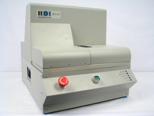
HDI SRA-FA Surface Reflectance Analyzer Product Description Used, good physical condition, HDI Instrumentation UPC-8000 / SRA-FA Surface Reflectance Analyzer and Controller. Acutal item shown, sold as pictured. Unit powered up but software password
Electronics Forum | Thu Sep 04 16:44:19 EDT 2003 | mleber
We are a military contractor running mixed technology CCA's. We currently "map" all defects off reflow and wave by indicating the defect on a map (plot from gerber) then passing it on to rework. The map is used for SPC data as well as overall perform
Electronics Forum | Tue Sep 16 19:16:11 EDT 2008 | hegemon
Hello everyone! > > I'm a student of electrical > engineering currently working on a thesis for my > BSc degree. It will be about post reflow AOIs and > AXIs, and I'd kindly like to ask you for some > help with it. > > I would like to know if t

Used SMT Equipment | X-Ray Inspection
• Nordson DAGE VR950 new technology, open, transmissive X-ray tube: -All voltages can reach <0.95 micron feature resolution – The highest voltage is 160KV, target power: 3W -Long service life of filament components -Automatic st
Used SMT Equipment | AOI / Automated Optical Inspection
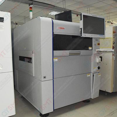
YAMAHA AOI YSi-V MACHINE KLT-000 1. Model: Yamaha ysi-v 2. Target substrate: l610 x w560 (maximum) ~ l50 x w50 (minimum) & supports l750mm super long substrate (optional) 3. Resolution: visible light (red/green/blue) & infrared (infra-
Industry News | 2018-04-17 21:06:54.0
SMTA is excited to announce the technical program has been finalized and registration is now open for the International Conference for Electronics Enabling Technologies. The event will be held June 5-7, 2018 in Markham, Ontario, Canada.
Industry News | 2012-10-26 07:25:15.0
Sechan Electronics, Inc.relationship with Aegis Software extends back over 11 years, beginning with their initial purchase of CircuitCAM and CheckPoint; software modules that are now integrated into iLaunch.

Parts & Supplies | SPI / Solder Paste Inspection
Quick programming, friendly programming interface Multiple measurement methods True one-button measurement Eight-way motion button, one-click focus Adjustable scanning pitch Solder paste 3D simulation function Powerful SPC function MARK
Technical Library | 2008-05-28 18:41:53.0
This paper describes correlation between a true 2D area measurement (e.g. printer) and a height map generated area from a SPI system. In addition, this paper will explore the correlation between area/volume measurements and bridge detection between 2D/3D techniques. The ultimate goal is to arm the process engineers with information that can be used to make decision that will impact defects, cost, throughput and Return On Investment.
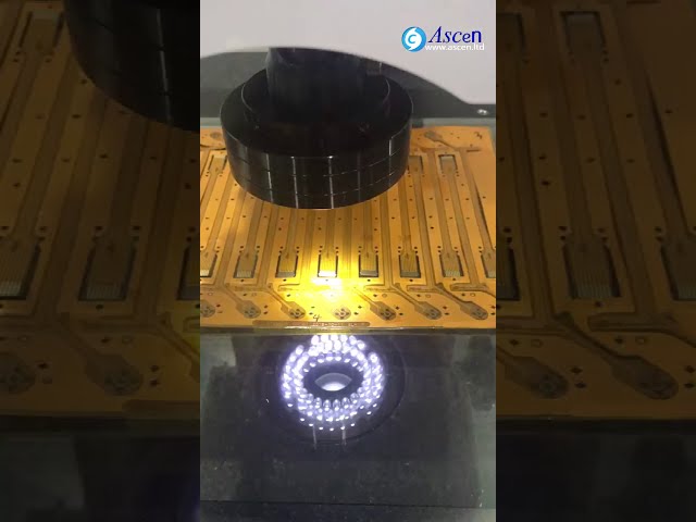
https://www.ascen.ltd/Products/PCB_board_assembly_system/vision_measurin/507.html Vision Measuring Machine and image measuring instrument can be used for dimensional accuracy measurement of various molds, aircraft, automobile, mobile phone, computer,
The new system delivers high-speed (5,700mm2/sec), high-accuracy (XY positioning of 3µm at 3?), height repeatability (below 2µm at 3?), and scalable resolutions of 7, 12 and 18µm for boards weighing 12kg. http://www.sakiglobal.com/automated-optical-i
Career Center | Auckland, New Zealand | Engineering
NAVMAN PCBA NPI Engineer Reporting To: PCBA NPI Technical Leader Primary Objective: Transition of PCBs from R&D design to a manufacturable state conforming to all facets of PCBA production Secondary: Develop DFM & best practice guidelines Res
Career Center | San DIego (Mira Mesa), California USA | Engineering,Maintenance,Production
Duties: Supports, develops and optimizes manufacturing processes. Reviews quality metrics to help produce high quality, repeatable processes. Assists with supporting and improving the SMT process (print process, placement, reflow, package-o
Career Center | toronto, toronto Canada | Engineering
Technical Skills • Plan, Design, Implement , Build Electronic Devices according to specifications • Inspect, Diagnose, Repair, Replace, Calibrate, Modified Electronic Devices • Use Blue Prints, Drawings, Diagrams, Measuring instruments Computer Ski
Career Center | Mysore, India | Engineering,Production,Quality Control,Technical Support
· New Product production line setup, Risk assessment, quality system deployment. · Process Engineering activities, PCB Design review w.r.t Design for manufacturability in Pilot lot. · Printed wiring Assembly Process Improvement (Stencil, PCB type, sc
Heller Industries Inc. | https://hellerindustries.com/wicking-defetcs/
× Re-printed in partnership with ITM Wicking Defects Defect: wicking A Wicking Defect is the flow of solder either up the lead of the component or along traces and possibly under insulation and through via holes
ASYMTEK Products | Nordson Electronics Solutions | https://www.nordson.com/en/divisions/sonoscan/support/application-notes/0202-pbga-3d-ami
. The Acoustic Solid above has not been sectioned yet. The spectrum-like feature at the left edge of the Acoustic Solid is the acoustic color map
.gif)


