
The PCB Footprint Expert is a powerful CAD library development tool powered by our own proprietary CAD LEAP Technology (Libraries Enhanced with Automated Preferences). It is packed with very powerful advanced library management features that cuts foo
New Equipment | Test Equipment
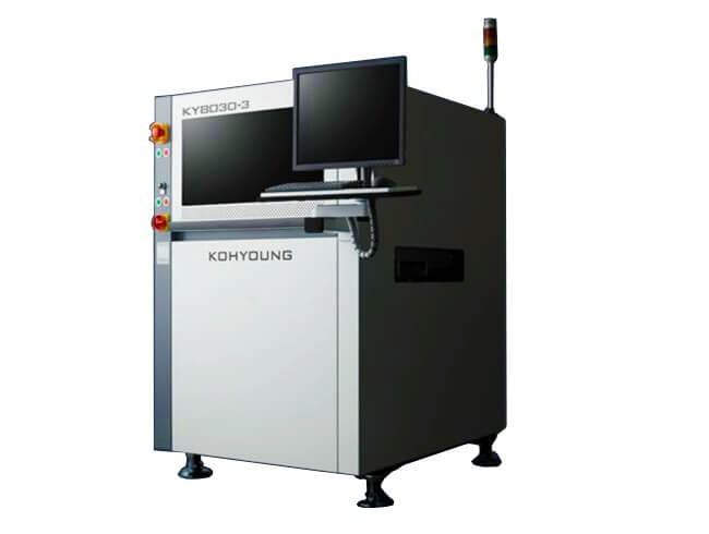
Koh Young KY8030-3 3D Inline SPI component Range: 01005 PCB size:350x330mm Dimension:1000x1335x1627mm weight:800kg Product description: Koh Young KY8030-3 3D Inline SPI, component Range: 01005, PCB size:350x330mm, Dimension:1000x1335x1627mm, weight:
Electronics Forum | Mon Jul 07 21:33:15 EDT 2014 | andrespena
The problem about covering it with glue (without using solder) is that the components might dislodge by a miniscule amount underneath the glue. So maybe the contact points will disconnect. I'm not sure if this will be a real problem, but if so it wo
Electronics Forum | Fri Jul 04 19:17:37 EDT 2014 | andrespena
Hi (I don't know if this forum is the best place to post something like this, but I don't know of other places on the internet, so... sorry if I'm in the wrong place) Might there be an easier way to add components (e.g. computer chips) to a circuit
Used SMT Equipment | Pick and Place/Feeders
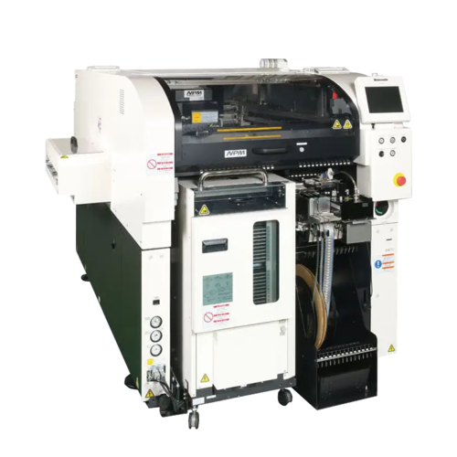
FEATURES ▶Higher productivity and quality with printing, placement and inspection process integration▶For larger boards and larger PCBs up to a size of 750 x 550 mm with component range up to L150 x W25 x T30 mm▶Higher area productivity through dual

Used SMT Equipment | Screen Printers
Dear Customer, We are please to offer you our machine as below: Model: MPM UP2000HiE -- 2 units Software Window NT Vintage: 2005 Flow Direction: Left to Right / Right to Left Rail Type: Front Fixed C/W Balance Controlled
Industry News | 2017-05-11 17:06:16.0
Library Expert Lite automatically builds footprints and 3D STEP models for tens of millions of parts, for free.
Industry News | 2020-11-06 17:34:05.0
Nano Dimension Ltd. (Nasdaq: NNDM) announced today that it will hold a webinar on Monday, Nov. 16, 2020 at 10 a.m. ET / 4 pm. CET.

Parts & Supplies | SPI / Solder Paste Inspection
Quick programming, friendly programming interface Multiple measurement methods True one-button measurement Eight-way motion button, one-click focus Adjustable scanning pitch Solder paste 3D simulation function Powerful SPC function MARK
Technical Library | 2020-03-26 14:55:29.0
This paper introduces line confocal technology that was recently developed to characterize 3D features of various surface and material types at sub-micron resolution. It enables automatic microtopographic 3D imaging of challenging objects that are difficult or impossible to scan with traditional methods, such as machine vision or laser triangulation.Examples of well-suited applications for line confocal technology include glossy, mirror-like, transparent and multi-layered surfaces made of metals (connector pins, conductor traces, solder bumps etc.), polymers (adhesives, enclosures, coatings, etc.), ceramics (components, substrates, etc.) and glass (display panels, etc.). Line confocal sensors operate at high speed and can be used to scan fast-moving surfaces in real-time as well as stationary product samples in the laboratory. The operational principle of the line confocal method and its strengths and limitations are discussed.Three metrology applications for the technology in electronics product manufacturing are examined: 1. 3D imaging of etched PCBs for micro-etched copper surface roughness and cross-sectional profile and width of etched traces/pads. 2. Thickness, width and surface roughness measurement of conductive ink features and substrates in printed electronics applications. 3. 3D imaging of adhesive dots and lines for shape, dimensions and volume in PCB and product assembly applications.

The PCB Footprint Expert is a powerful CAD library development tool powered by our own proprietary CAD LEAP Technology (Libraries Enhanced with Automated Preferences). It is packed with very powerful advanced library management features that cuts foo
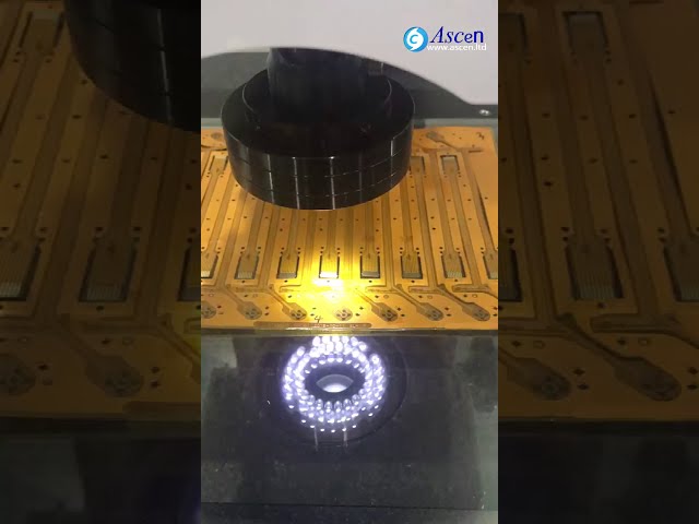
https://www.ascen.ltd/Products/PCB_board_assembly_system/vision_measurin/507.html Vision Measuring Machine and image measuring instrument can be used for dimensional accuracy measurement of various molds, aircraft, automobile, mobile phone, computer,
Career Center | Tucson, Arizona USA | Quality Control
For over 30 years VSC, an independent subsidiary of Verify, Inc., has been a trusted resource to over 200 companies in aerospace, defense, and high-technology industries. This partnership has created worldwide opportunities for contract Project Speci
SMTnet Express, March 26, 2020, Subscribers: 35,188, Companies: 10,983, Users: 25,722 New High-Speed 3D Surface Imaging Technology in Electronics Manufacturing Applications Credits: FocalSpec, Inc. This paper introduces line confocal technology
KingFei SMT Tech | https://www.smtspare-parts.com/sale-40867101-cn-m-tn-printing-machine-corner-machine.html
CN-M-TN Printing Machine Corner Machine Product Details: Place of Origin: Japan Brand Name: Corner machine Model Number: CN-M-TN Payment & Shipping Terms: Minimum Order Quantity
| https://www.smtfactory.com/I-C-T-V5000H-3D-AOI-Optical-Inspection-Machine-For-PCB-pd49400944.html
I.C.T-V5000H | 3D AOI Optical Inspection Machine For PCB from China manufacturer - I.C.T SMT Machine English Türk dili Tiếng Việt 한국어 日本語 Italiano Deutsch


winsouce.jpg)