
Industry Directory | Other / Consultant / Service Provider / Media / Publisher / Online Resource
PCB Libraries' "Footprint Expert" suite uses CAD LEAP(tm) Technology to greatly simplify footprint and 3D STEP model creation; it is used by tens of thousands of PCB designers and engineers all over the world.

Industry Directory | Other / Consultant / Service Provider / Manufacturer
ScanCAD is an industry leader in inspection, measurement, process control and reverse engineering. Our solutions support OEM's, manufacturers, stencil fabricators, repair depots, and others in optimizing quality and yield.
New Equipment | Rework & Repair Equipment
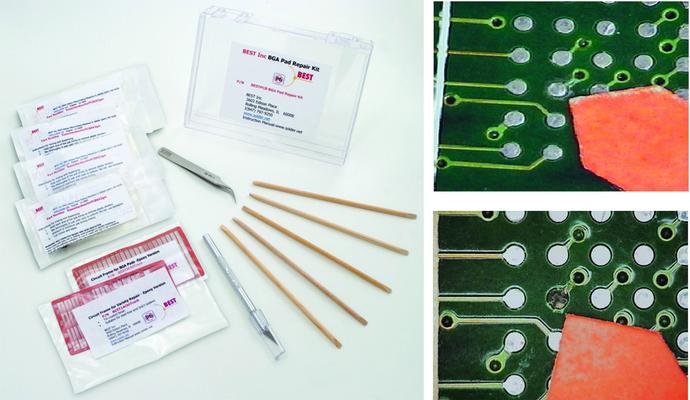
The BEST PCB pad repair repair kit gives you the tools you need for fast modification and repair of PCB circuit pads-no matter what their size. Our online PCB repair training videos, our master instructors along with these materials allows you to mee

New Equipment | Rework & Repair Equipment
The BEST PCB Epoxy Repair Kit can be used to repair lifted pads and traces as well as build up and repair edge corner damage to PCBs or repair solder mask which has been damaged or removed. By adding colorants a pcb color epoxy kit can be made up cus
Electronics Forum | Thu Feb 12 20:42:10 UTC 2026 | SMTA-64387381
Is there any good reason not to print solder paste on DNPs on ENIG plated PCBs? Want to use a single stencil for building several BOM configurations on a common PCB. The in house design team is saying they do not allow printing on the DNP pads.
Used SMT Equipment | In-Circuit Testers
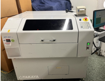
Description Make: Takaya Model: APT-9411CE Year: 2010 Type: Flying Probe Details: Takaya APT 9411 CE Flying Probe The APT-9411CE is designed for users who are looking for a precise and reliable test system with an easy to use softwar
Used SMT Equipment | Screen Printers
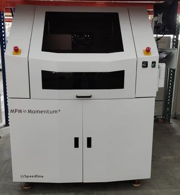
Momentum is designed to provide efficiency and speed. With its triple track conveyor rails and servo drive motors, for example, the Momentum Elite model orders the highest performance capacity in the series, making it the ideal printer for high volum
Industry News | 2003-06-17 08:07:40.0
The Radiall SMT coupler range now includes the new 14.2 x 5.1mm mini type.
Industry News | 2009-10-17 09:43:47.0
Reduce PCB Repair Costs

Technical Library | 2019-05-29 01:47:22.0
1.Vias near SMD pads: Solder can flow into the via after melted. As a result cold joint will appear in the end. Check the picture below. 2.Vias on SMD pads: Solder can flow into the via more easier after melted. Check the picture below. 3.Via opening without soldermask covered. When workers solder TH parts by hand, soldering iron can touch vias sometime, then tiny amounts molten solder will stay on vias. This can lead to electrical short easily. We recommend you make all vias tenting (covered by solder mask) if it is possible.
PCBNPI-Professional PCB Fab/PCB Assembly Service Provider From China
Technical Library | 2023-05-02 19:06:43.0
As 0402 has become a common package for printed circuit board (PCB) assembly, research and development on mounting 0201 components is emerging as an important topic in the field of surface mount technology for PWB miniaturization. In this study, a test vehicle for 0201 packages was designed to investigate board design and assembly issues. Design of Experiment (DOE) was utilized, using the test vehicle, to explore the influence of key parameters in pad design, printing, pick-andplace, and reflow on the assembly process. These key parameters include printing parameters, mounting height or placement pressure, reflow ramping rate, soak time and peak temperature. The pad designs consist of rectangular pad shape, round pad shape and home-based pad shape. For each pad design, several different aperture openings on the stencil were included. The performance parameters from this experiment include solder paste height, solder paste volume and the number of post-reflow defects. By analyzing the DOE results, optimized pad designs and assembly process parameters were determined.

PCB pad repair technique demonstrated using the 2-part epoxy method. More on this PCB pad repair technique: http://www.solder.net/services/pcb-repair/pad-and-trace-repair/ More on the recommended epoxy: http://www.soldertools.net/pcb-repair-epoxy-r

This video is on the dry film pad repair technique per IPC 7721 standards. BEST professional instructors demonstrate the proper technique for the repair for PCB pads using the dry film. http://www.solder.net More on PCB pad repair here: http://www.s
Training Courses | ON DEMAND | | PCB Rework and Hand Soldering Courses
The PCB rework and hand soldering courses courses cover techniques of rework and repair of PCBs, BGAs and other electronics assemblies, and teach fundamentals of soldering of electronics assemblies.
Training Courses | ON DEMAND | | PCB Rework and Hand Soldering Courses
The PCB rework and hand soldering courses courses cover techniques of rework and repair of PCBs, BGAs and other electronics assemblies, and teach fundamentals of soldering of electronics assemblies.
Events Calendar | Tue Apr 19 18:30:00 UTC 2022 - Tue Apr 19 18:30:00 UTC 2022 | ,
Virtual Course: Selection Criteria of Surface Finish for Next Generation PCB Technologies
Events Calendar | Tue May 30 18:30:00 UTC 2023 - Tue May 30 18:30:00 UTC 2023 | Holtsville, New York USA
Long Island Chapter Meeting: Fine Feature Paste Printing, Stencil Design and Solder Technology
Career Center | Sherman, Texas USA | Engineering,Production,Research and Development,Technical Support
SMT Packaging Engineer: Location: Texas - Sherman , TX Group: HVAL Degree Requirements: BS ME/ChemE/Materials The person in this position will have the ability to make very significant financial contributions to TI because this is a very critic
Career Center | Lincoln, Nebraska USA | Engineering
Brief Description of Job Duties: Provide new program engineering support with emphasis on technical SMT process development. Key activities would include recommendations and implementation of components, SMT pad design, solder methods, testing and r
Career Center | , NEW DELHI India | Engineering
Background includes a proven record of education, experience, and technical strengths in electronic circuit design and troubleshooting, software development, and versatility in operating systems. � Engineering experience working with designers, mark
Career Center | Newport Beach, California USA | Engineering,Management,Production
KEVIN RAGER P.O.BOX 7878, NEWPORT BEACH, 949 922 8997, KEVIN.RAGER@EDA-INC.US OBJECTIVE I am trying to find a consistent work flow that provides mentally challenging yet stimulating experiences in design and prototype development. EXPERIENCE 1997
PCB Libraries, Inc. | https://www.pcblibraries.com/Forum/how-to-calculate-dpak-thermal-pad-size_topic2707_post11014.html
How to calculate DPAK Thermal pad size? - PCB Libraries Forum Forum Home > Training / Events > PCB Design Basics New Posts FAQ Search Events Register Login How to calculate DPAK Thermal pad size
Imagineering, Inc. | https://www.pcbnet.com/blog/considerations-for-pcb-board-design-layout/
Considerations for PCB Board Design & Layout | Imagineering, Inc. Skip to main content Resources Support Contact Us FAQs Live Chat My Account 847-806-0003 Menu PCB Capabilities Fabrication Technology Roadmap Materials Available HDI Tolerances Certifications


