
Industry Directory | Consultant / Service Provider / Media / Publisher / Online Resource / Other
PCB Libraries' "Footprint Expert" suite uses CAD LEAP(tm) Technology to greatly simplify footprint and 3D STEP model creation; it is used by tens of thousands of PCB designers and engineers all over the world.
Industry Directory | Consultant / Service Provider / Manufacturer
We are a CEM and PADS Layout service bureau. We are liquidating quality assembly equipment.

The PCB Footprint Expert is a powerful CAD library development tool powered by our own proprietary CAD LEAP Technology (Libraries Enhanced with Automated Preferences). It is packed with very powerful advanced library management features that cuts foo

New Equipment | Design Services
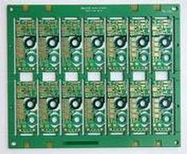
All kinds EMI/EMS Solutions. EMI/EMS Applications in all nations. Safety Applications in all nations. Types of Rigid, Flex, Rigid-flex and HDI. Layer design from single up to 24. Product debug and remodeling. Design for EMC - reduced EMI
Electronics Forum | Fri Nov 17 15:04:59 EST 2006 | ehess
WE have a problem with a DPAK component floating during reflow, causing it to move to the point where it affects the toe fillet. We have been using a dot of SMT epoxy to hold it secure for the moment. I have looked on many sites, but no whrere can
Electronics Forum | Mon Nov 20 20:38:21 EST 2006 | davef
�IPC-7351 LP Wizard� is the library maintenance tool that is revolutionizing the way designers work. The IPC-7351 LP family tools can give you access to options that will allow you to quickly and easily browse your PCB land pattern library to locate,
Industry News | 2010-07-22 22:37:02.0
IPC — Association Connecting Electronics Industries® has released the B revision of IPC-7351, Generic Requirements for Surface Mount Design and Land Pattern Standard. The leading industry standard for surface mount land pattern design and layout, IPC-7351B provides designers and printed board fabricators with updated guidance on requirements of land pattern geometries used for the surface attachment of electronic components, as well as surface mount design recommendations for achieving the best possible solder joints.
Parts & Supplies | Circuit Board Assembly Products
PULANG TECHNOLOGY CO,.LTDOffers electronic manufacturing services including PCB designing, electronic contract manufacturing including electronic product design, electronic product development, electronic product repair, PCB manufacturing, electronic
Technical Library | 2023-05-02 19:03:34.0
The demand for 0201 components in consumer products will increase sharply over the next few years due to the need for miniaturization. It is predicted that over 20 billion 0201 components will be used in more than one billion cell phones worldwide by the year 2003. Therefore, research and development on 0201 assembly is becoming a very hot topic. The first step to achieve a successful assembly process is to obtain a good PCB design for 0201 packages. This paper presents the data and criteria of PCB design for 0201 packages, including the pad design for 0201 components, and the minimum pad spacing or component clearance between 0201 components or between 0201 and other components. A systematic study on pad design and pad spacing was undertaken, using two test vehicles and three Design of Experiments (DOEs). In the first DOE, 2 out of 18 types of 0201 pad designs were selected based on process yield. The second DOE was focused on pad spacing, including 10mil, 8mil, 6mil and 4mil. The third experiment was final optimization, using two types of optimized pad designs with 10mil, 8mil and 6mil pad spacing. Through the above experiments, the design guideline for PCB layout for 0201 packages and the assembly process capability are identified.
Technical Library | 2009-05-14 13:57:43.0
Is screen printing technology able to keep pace with rising quality demands and increasingly complex board layouts? Or, is new jet printing technology ready to fill the gap? A comparison study between the two methods reveals some interesting differences. Screen printers offer some possibilities for optimizing solder paste deposits, but optimization is far easier and quicker with the jet printer. At the same time, the ability to print individualized deposits on every single pcb pad may be the ultimate answer to the growing quality challenge.

The PCB Footprint Expert is a powerful CAD library development tool powered by our own proprietary CAD LEAP Technology (Libraries Enhanced with Automated Preferences). It is packed with very powerful advanced library management features that cuts foo

See what some of our customers have to say about the complete PCB design environment offered by PADS 9.0. This next generation in PCB Design tool combines an intuitive, flexible design environment with integrated, scalable technology. Giving engine
Career Center | Sherman, Texas USA | Engineering,Production,Research and Development,Technical Support
SMT Packaging Engineer: Location: Texas - Sherman , TX Group: HVAL Degree Requirements: BS ME/ChemE/Materials The person in this position will have the ability to make very significant financial contributions to TI because this is a very critic
Career Center | Wellsboro, Pennsylvania USA | Engineering
SMT PROCESS ENGINEER: (Wellsboro, PA) - Designs, defines and plans the manufacturing process. Specifies and directs installation of new processes. Plans equipment build schedules and monitors vendor progress. Defines and recommends equipment, methods
Career Center | Newport Beach, California USA | Engineering,Management,Production
KEVIN RAGER P.O.BOX 7878, NEWPORT BEACH, 949 922 8997, KEVIN.RAGER@EDA-INC.US OBJECTIVE I am trying to find a consistent work flow that provides mentally challenging yet stimulating experiences in design and prototype development. EXPERIENCE 1997
Imagineering, Inc. | https://www.pcbnet.com/blog/considerations-for-pcb-board-design-layout/
Considerations for PCB Board Design & Layout | Imagineering, Inc. Skip to main content Resources Support Contact Us FAQs Live Chat My Account 847-806-0003 Menu PCB Capabilities Fabrication Technology Roadmap Materials Available HDI Tolerances Certifications
| https://www.eptac.com/faqs/ask-helena-leo/ask/solder-touching-glass-body-components-like-diodes
. The reasoning is the same, thermal shock to the component. I realize this is a difficult thing to observe, but the design of the product has to be specific in the pad layout design to minimize and eliminate this condition from occurring


