Industry Directory | Manufacturer
US manufacturer of metallized ceramic substrates & packages; specializing in PCTF (plated copper over thick film) & low cost AgENIG (silver with electroless nickel and immersion gold plating).
High Tech, Quick Turn, Manufacturer of PCB's up to 44 layer count. Specializing in Prototype and R&D. Mil-Spec 31032 & 55110 Certified. Located in Fremont, CA & Amesbury, MA.
New Equipment | Education/Training
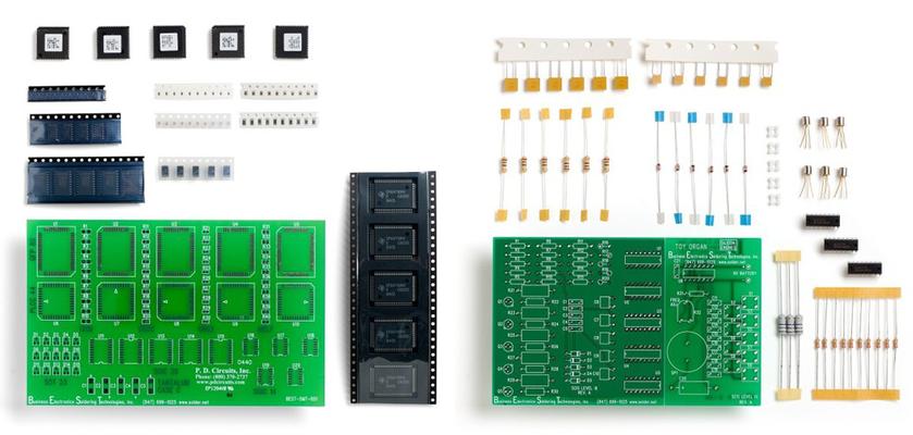
BEST training kits feature REAL circuit boards that represent actual soldering conditions. These training kits feature ".062 thick multilayer boards which are more representative of the thermal conditions of "real" circuit boards. This board feature
New Equipment | Rework & Repair Equipment
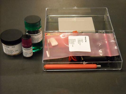
The BEST Gold Contact Replating Kit includes the tools you need for fast replating and modification of circuit contacts. Edge contacts may require replating if they are contaminated with solder or become scratched during handling or do not meet the m
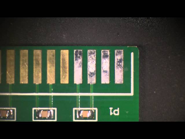
Electronics Forum | Thu Jul 15 13:27:42 EDT 2010 | xps
Thanks... anyway I confirm, the nickel disappear (verified by cross section)and a strange substance greyish above gold, covering the tabs after test. I don't know the reason for this phenomenon. I don't believe that with proper electrolytic nickel fi
Electronics Forum | Wed Nov 30 06:23:32 EST 2005 | wmeyers
Thanks Dave! Bill
Industry News | 2003-05-19 10:06:43.0
The PCB is available with a maximum panel size of 406-by-460mm and a minimum board thickness of 0.8mm.
Industry News | 2003-03-21 08:12:24.0
Tecan reckons it is consistently producing what may be regarded as the most efficient stencils in the world today.
Parts & Supplies | Circuit Board Assembly Products
1). FR-4 Tg 170 + Rogers 4350B 2). 290*130mm/1up 3). 6 layers at 1.6mm thick 4). Green solder mask/White ident 5). 35um copper finished, ED copper. 6). Electroless gold. 7). Countersunk slots.
Parts & Supplies | Circuit Board Assembly Products
1) 160*100mm, FR-4 CTI ≥ 600V 2) 8 layer impedance control 3) Copper weight(finished inner/outer): 1 oz 4) LPI Green mask/white silk 5) Min hole 0.19mm, 5/3 track/gap 6) 1.6mm +/-10% thick 7) Immersiong gold over nickel
Technical Library | 2014-11-06 16:43:24.0
This paper summarizes the results of recent investigations to examine the effect of electroless nickel process variations with respect to Pb-free (Sn-3.0Ag-0.5Cu) solder connections. These investigations included both ENIG and NiPd as surface finishes intended for second level interconnects in BGA applications. Process variations that are suspected to weaken solder joint reliability, including treatment time and pH, were used to achieve differences in nickel layer composition. Immersion gold deposits were also varied, but were directly dependent upon the plated nickel characteristics. In contrast to gold, different electroless palladium thicknesses were independently achieved by treatment time adjustments.
Technical Library | 2014-08-07 15:13:44.0
Gold embrittlement in SnPb solder is a well-known failure mechanism in electronic assembly. To avoid this issue, prior studies have indicated a maximum gold content of three weight percent. This study attempts to provide similar guidance for Pb-free (SAC305) solder. Standard surface mount devices were assembled with SnPb and SAC305 solder onto printed boards with various thicknesses of gold plating. The gold plating included electroless nickel immersion gold (ENIG) and electrolytic gold of 15, 25, 35, and 50 microinches over nickel. These gold thicknesses resulted in weight percentages between 0.4 to 7.0 weight percent.
BEST Inc master instructor Norman Mier demonstrates how to replate gold fingers using the BEST gold contact replating kit. In this video he demonstrates how to repair, prepare and replate the finger using a gold replating solution. If you want to lea
Events Calendar | Wed Apr 20 00:00:00 EDT 2022 - Wed Apr 20 00:00:00 EDT 2022 | ,
Virtual Course: Selection Criteria of Surface Finish for Next Generation PCB Technologies
Events Calendar | Wed Mar 18 00:00:00 EDT 2020 - Wed Mar 18 00:00:00 EDT 2020 | College Park, Maryland USA
CALCE Reliability Science Symposium - Spring 2020
SMTnet Express, November 6, 2014, Subscribers: 23500, Members: Companies: 14091, Users: 37109 Effect of Process Variations on Solder Joint Reliability for Nickel-based Surface Finishes Hugh Roberts, Sven Lamprecht, Gustavo Ramos, Christian Sebald
| https://www.eptac.com/soldertips/soldertips-solderability-issues-with-nickle-plated-surfaces/
. They will re-tin with flux, but reappear following steam-aging. Is this something you have encountered before? Answer: There is a metallurgy issue with soldering to nickel plated surfaces and depending upon the thickness of the final tin/lead coating, the steam aging will penetrate the finish coating and create a
ORION Industries | http://orionindustries.com/pdfs/Electrically_conductive_poron.pdf
#180-034 EC-2000 SERIES CONDUCTIVE SILICONES High Performance Foams 171 West St. Charles Road Carol Stream, IL 60188-2081 Tel: 630.784.6200 / Fax: 630.784.6201 www.rogerscorporation.com Technical Data TYPICAL PROPERTIES Test Method Filler Base Polymer Specific Gravity, g/cc Thickness


