Industry Directory | Manufacturer
SMT Rework & Repair BGA Replacement BGA Rework BGA X-Ray Services Component replacement Outsourced Board Level Repair and Assembly Contractor Sub-Contractor Open to all opportunities. Don't hesitate
Industry Directory | Manufacturer's Representative
SMT assembly equipment including placement, reflow & vapor phase soldering, cleaning, X-Ray, AOI, SPI, conveyors. First Article Inspection (FAI). Consumables, splicing systems & tools, splice tape & clips. Understencil wiping Roll
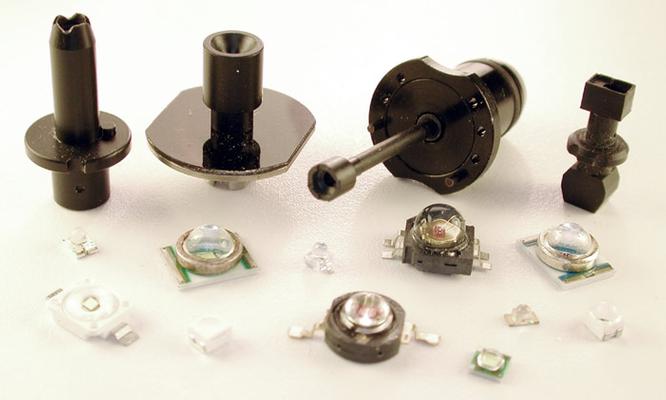
Count On Tools specializes in custom engineered nozzles for all types of LEDs (Cree, Luxeon, Phillips, NIchia, Osram, etc). Recent growth in LED technology and solid state lighting has provided the electronics manufacturing industry with viable sol

Mantis Compact is an ergonomic, low fatigue visual inspection microscope, excelling in the low magnification range for PCB inspection tasks where bench magnifiers have traditionally been used. Featuring Vision Engineering's patented eyepiece-less te
Electronics Forum | Thu Dec 01 21:15:26 EST 2005 | davef
Try: * Caltex [www.bgascope.com] "Hirox" scope * ERSA [www.ersa.de] Ersascope
Electronics Forum | Tue Dec 06 22:48:04 EST 2005 | minimicro
Mike You are my hero. A real world person.
Used SMT Equipment | Semiconductor & Solar
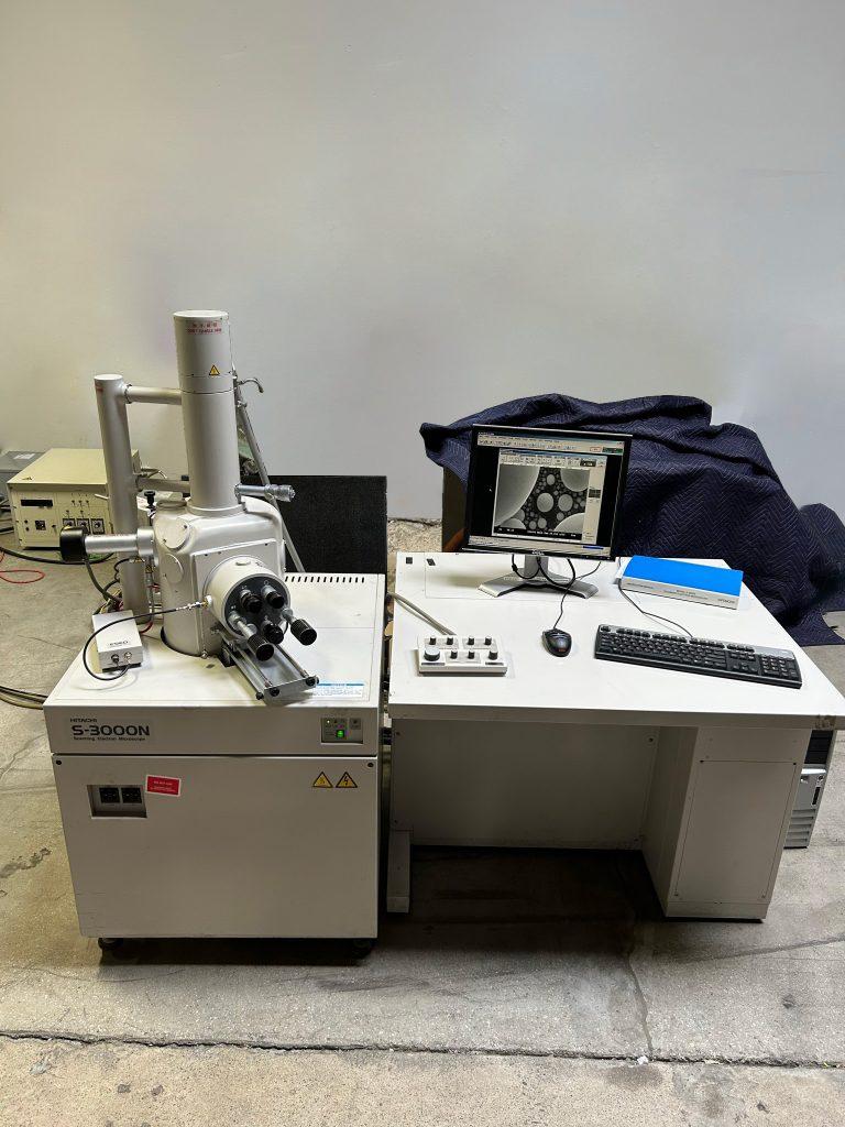
HITACHI S-3000-N Scanning Electron Microscope (SEM) Not sure of vintage! Full specifications upon request. https://www.karenmadison.com/hitachi-s-3000-n-scanning-electron-microscope-sem/
Used SMT Equipment | General Purpose Equipment
Bonder appears to be in quite nice cosmetic condition, showing some signs of normal wear. Being sold refurbished and in working condition, with a 30-day parts warranty to the contiguous US 48 states only. 2 to 4 weeks allowance for refurbishm
Industry News | 2003-04-21 08:46:05.0
Kaisertech has added Meiji Techno microscopes and vision equipment to its range of electronic production equipment.
Industry News | 2003-07-09 09:00:46.0
He will have responsibility for all aspects of Photronics� manufacturing and sales activities in China, Singapore and Taiwan.
Parts & Supplies | Assembly Accessories
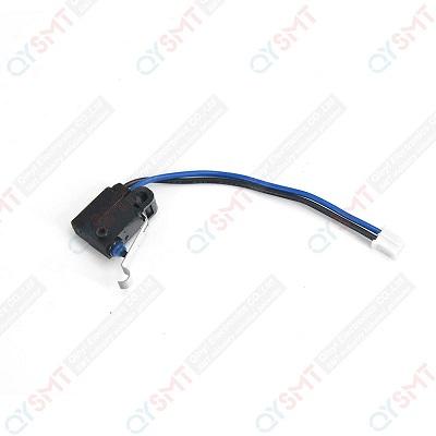
FUJI-sw-micro-PZ02394 electron microscope 3.5-90X Magnification HD HDMI/USB 14MP Camera electron microscope 3.5x-90x stereo microscope MICRO EJECTOR UNIT KM8-M7162-00 MICRO PHOTO SENSOR THETA-AXIS J3212027A J3212027A Micro Switch S5

Parts & Supplies | Pick and Place/Feeders
The definition of SMT SMT is the surface assembly technology,surface mount technology(surface mount technology)(Surface Mounted Technology abbreviation),is currently the most popular electronic assembly industry,a technology and technology. What a
Technical Library | 2014-07-02 16:46:09.0
Growth behaviors of intermetallic compounds (IMCs) and Kirkendall voids in Cu/Sn/Cu microbump were systematically investigated by an in-situ scanning electron microscope observation. Cu–Sn IMC total thickness increased linearly with the square root of the annealing time for 600 h at 150°C, which could be separated as first and second IMC growth steps. Our results showed that the growth behavior of the first void matched the growth behavior of second Cu6Sn5, and that the growth behavior of the second void matched that of the second Cu3Sn. It could be confirmed that double-layer Kirkendall voids growth kinetics were closely related to the Cu–Sn IMC growth mechanism in the Cu/Sn/Cu microbump, which could seriously deteriorate the mechanical and electrical reliabilities of the fine-pitch microbump systems
Technical Library | 2021-09-21 20:36:45.0
The present paper gives an overview of surface failures, internal nonconformities and solders joint failures detected by microscopic analysis of electronic assemblies. Optical microscopy (stereomicroscopy) and Fourier-Transform- Infrared (FTIR) microscopy is used for documentation and failure localization on electronic samples surface. For internal observable conditions a metallographic cross-section analysis of the sample is required. The aim of this work is to present some internal and external observable nonconformities which frequently appear in electronic assemblies. In order to detect these nonconformities, optical microscopy, cross section analysis, FTIR-microscopy and scanning electron microscopy with energy dispersive spectrometry (SEM-EDS) were used as analytical techniques.

ACI Technologies Inc. (ACI) is a scientific research corporation dedicated to the advancement of electronics manufacturing processes and materials for The Department of Defense and industry. This video provides an overview of our commercial service

The BEST Mobile Training Center (MTC) is the only self-contained solder training center on wheels. We can just pull up to your facility with everything you need for training! The MTC has been all across the continental United States. It has all of th
Training Courses | | | Other Courses
Other courses related to electronics manufacturing and assembly
Career Center | Buffalo Grove, Illinois USA | Engineering,Production
SMT Soldering Surface Mount and Through Hole, hand soldering. Must be experienced in reading parts lists and know how to identify electronics components. Job requires use of a microscope and/or a maginfying glass.
Career Center | San Juan Capistrano, Arizona USA | Sales/Marketing
Sales Engineer position with nationwide Manufacturers' Representative selling Production Supplies, Soldering equipment, SMT Pick & Place, AOI, ESD, Microscopes, Storage and Handling systems. Knowledge of electronics industry, excellent presentati
Career Center | , California | Quality Control
Tammy T Vo P.O. Box 2213 (714) 254-5073 E-mail: nhutamvo@yahoo.com Position of Interest Senior Quality Inspector Aerospace Manufacturing. / Electronic PCBA/Advanced coating technologies Profile of Qualifications 12 years of experience wo
Career Center | Fremont, California USA | Engineering,Production
4 years of PCB assembly process.
advancement of flexible wearable electronics allows sig
Heller Industries Inc. | https://hellerindustries.com/wp-content/uploads/2018/07/pan_APEX06.pdf
). The fracture surfaces have been studied using a scanning electron microscopy (SEM) with energy dispersive spectroscopy (EDS). Introduction The increasing awareness of health risk associated with lead (Pb


