Industry Directory | Manufacturer
Pemtron develops and manufactures 3-D Solder Paste Inspection, 3-D Nano Profilers and Scanning Electron Microscopes
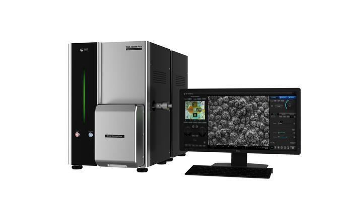
SNE-4500M Plus The Highest-end Tabletop SEM Cost-effective Table-top SEM with Max. 150,000x of magnification by miniaturizing modules. Able to scan images with high resolution of 5nm by the installation of the variable aperture with ease of us
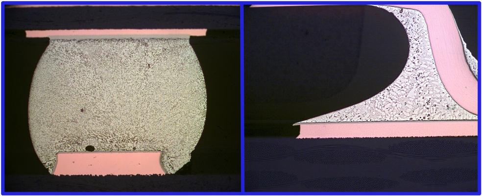
Please visit our main microsectional analysis page for more information. Process Sciences uses microsection for both failure analysis and process validation. Our cross sections reveal intermetallic layers, defects, and other physical characteristic
Electronics Forum | Fri Dec 09 13:01:16 EST 2005 | Amol Kane
why in the world would you have a fax controller board electron microscoped?
Electronics Forum | Thu Mar 27 14:09:41 EST 2003 | Enrique Chairez
Hi All, I have observed this problem with one PCB supplier, the portion of the PCB area affected was cut and observed in SEM (Scanning Electron Microscope) and submitted to an EDX (Energy Disperse X ray analysis), finding Phosphorus levels higher
Used SMT Equipment | Semiconductor & Solar
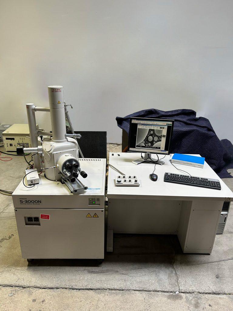
HITACHI S-3000-N Scanning Electron Microscope (SEM) Not sure of vintage! Full specifications upon request. https://www.karenmadison.com/hitachi-s-3000-n-scanning-electron-microscope-sem/
Industry News | 2014-05-14 16:54:20.0
A newly released training video, DVD-166C, “Counterfeit Components” from IPC — Association Connecting Electronics Industries®, explains not only how counterfeit components find their way into the supply chain, but more important, how to detect fraudulent devices during visual inspection.
Industry News | 2017-04-05 11:18:26.0
Microtronic GmbH is pleased to announce that it has added the PEMTRON PS™ Series Scanning Electron Microscopes (SEMs) to its product line up in parts of the EU. The PS Series Models include the PS-210 Compact Desk Top Mini-SEM, the PS-230 High Performance Normal-SEM, and PS-250 Analytical Normal-SEM.
Parts & Supplies | Assembly Accessories
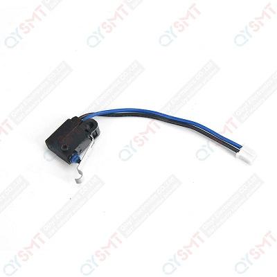
FUJI-sw-micro-PZ02394 electron microscope 3.5-90X Magnification HD HDMI/USB 14MP Camera electron microscope 3.5x-90x stereo microscope MICRO EJECTOR UNIT KM8-M7162-00 MICRO PHOTO SENSOR THETA-AXIS J3212027A J3212027A Micro Switch S5
Technical Library | 2014-07-02 16:46:09.0
Growth behaviors of intermetallic compounds (IMCs) and Kirkendall voids in Cu/Sn/Cu microbump were systematically investigated by an in-situ scanning electron microscope observation. Cu–Sn IMC total thickness increased linearly with the square root of the annealing time for 600 h at 150°C, which could be separated as first and second IMC growth steps. Our results showed that the growth behavior of the first void matched the growth behavior of second Cu6Sn5, and that the growth behavior of the second void matched that of the second Cu3Sn. It could be confirmed that double-layer Kirkendall voids growth kinetics were closely related to the Cu–Sn IMC growth mechanism in the Cu/Sn/Cu microbump, which could seriously deteriorate the mechanical and electrical reliabilities of the fine-pitch microbump systems
Technical Library | 2015-02-12 16:57:56.0
Electronic systems are known to be affected by the environmental and mechanical conditions, such as humidity, temperature, thermal shocks and vibration. These adverse environmental operating conditions, with time, could degrade the mechanical efficiency of the system and might lead to catastrophic failures.The aim of this study is to investigate the mechanical integrity of lead-free ball grid array (BGA) solder joints subjected to isothermal ageing at 150°C for up to 1000 hours. Upon ageing at 150°C the Sn-3.5Ag solder alloy initially age-softened for up to 200 hours. This behaviour was linked to the coarsening of grains. When aged beyond 200 hours the shear strength was found to increase up to 400 hours. This age-hardening was correlated with precipitation of hard Ag3Sn particles in Sn matrix. Further ageing resulted in gradual decrease in shear strength. This can be explained as the combined effect of precipitation coarsening and growth of intermetallic layer. The fractured surfaces of the broken solder balls were also investigated under a Scanning Electron Microscope. The shear failures were generally due to ductile fractures in bulk solders irrespective of the ageing time.
![[SEC] SEM(Scanning Electron Microscope) SNE 4500M Plus Premium Version of Highest-end](https://img.youtube.com/vi/C9ny0wTR8mY/sddefault.jpg)
#SEM#SEC#??????? Model: SNE-4500M Plus (A) / (B) Resolution: 5nm (30kV, SE Image) Magnification: 30x~150,000x Detector: Secondary Electron(SE) / Backscattered Electron(BSE) Vacuum: High / Low Stage: X,Y, Z, R, T : Fully motorized Navigation mode wi
Heller Industries Inc. | https://hellerindustries.com/wp-content/uploads/2018/07/pan_APEX06.pdf
). The fracture surfaces have been studied using a scanning electron microscopy (SEM) with energy dispersive spectroscopy (EDS). Introduction The increasing awareness of health risk associated with lead (Pb


winsouce.jpg)