Industry Directory | Manufacturer
Additive modifies bare PCBs by adding solid copper traces, SMT Pads and deletes even under BGAs. RoHS / non-RoHS bare boards when engineering changes are needed and re-design is not done. Improve quality, thru-put and reliabilty while lowering cost.
Industry Directory | Manufacturer
Speedy Circuits manufactures technically demanding PCBs, flex & rigid-flex circuits, metal core boar
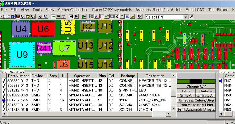
If you have only Gerber data files to work with then ProntoGERBER-CONNECTION can help you! ProntoGERBER-CONNECTION imports raw Gerber data and allows the user to add intelligent information to the shapes on the display and create process assembly

The PCB Footprint Expert is a powerful CAD library development tool powered by our own proprietary CAD LEAP Technology (Libraries Enhanced with Automated Preferences). It is packed with very powerful advanced library management features that cuts foo
Electronics Forum | Sat Oct 21 03:55:14 EDT 2000 | DL
Dennis, I've seen this before, and in our case we didn't need to seal the edges because there was no concern of shorting or anything in the end product, this is a choice you will have to make, Does your end product have any protrusions or mounting h
Electronics Forum | Fri Oct 20 14:13:32 EDT 2000 | DENNIS XIONG
Dear all, We have a PCB design mistake that causes exposed copper layers on the edges of breakaway locations. Although we fixed the design, but we already made a lot of boards plus many made before we found the problem. I wonder if any one have some
Industry News | 2014-10-01 15:59:00.0
PCB provider Cirtech Electronics located in Cape Town, South Africa will be liquidating their assets utilizing the online auction services of GoIndustry and Baja Bid. Bidding for the auction will open promptly at 8:00am PDT on October 7th, 2014 and will begin closing at 6:00am PDT on October 14th, 2014.
Industry News | 2014-10-10 16:27:51.0
CB provider Cirtech Electronics will be liquidating their assets utilizing the online auction services of GoIndustry and Baja Bid.
Parts & Supplies | Circuit Board Assembly Products
Specifications 1.One-stop OEM pcb assembly service. 2.ROHS, SGS, UL certificated 3.Reasonable price 4.High Quality 5.Fast Delivery PCB Assembly&PCBA Service 1. Experienced components sourcing team specially for scarce parts 2.1 to 12 layers m
Parts & Supplies | Circuit Board Assembly Products
Specifications 1.One-stop OEM pcb assembly service. 2.ROHS, SGS, UL certificated 3.Reasonable price 4.High Quality 5.Fast Delivery PCB Assembly&PCBA Service 1. Experienced components sourcing team specially for scarce parts 2.1 to 12 layers m
Technical Library | 2021-11-03 16:52:47.0
This paper proposes the integration of pulsed photonic sintering into multi-material additive manufacturing processes in order to produce multifunctional components that would be nearly impossible to produce any other way. Pulsed photonic curing uses high power Xenon flash lamps to thermally fuse printed nanomaterials such as conductive metal inks. To determine the feasibility of the proposed integration, three different polymer additive manufacturing materials were exposed to typical flash curing conditions using a Novacentrix Pulseforge 3300 system. FTIR analysis revealed virtually no change in the polymer substrates, thus indicating that the curing energy did not damage the polymer. Next, copper traces were printed on the same substrate, dried, and photonically cured to establish the feasibility of thermally fusing copper metal on the polymer additive manufacturing substrates. Although drying defects were observed, electrical resistivity values ranging from 0.081 to 0.103 Ω/sq. indicated that high temperature and easily oxidized metals can be successfully printed and cured on several commonly used polymer additive manufacturing materials. These results indicate that pulsed photonic curing holds tremendous promise as an enabling technology for next generation multimaterial additive manufacturing processes.
Technical Library | 2024-07-24 01:04:35.0
Quad Flat No Leads (QFN) package designs receive more and more attention in electronic industry recently. This package offers a number of benefits including (1) small size, such as a near die size footprint, thin profile, and light weight; (2) easy PCB trace routing due to the use of perimeter I/O pads; (3) reduced lead inductance; and (4) good thermal and electrical performance due to the adoption of exposed copper die-pad technology. These features make the QFN an ideal choice for many new applications where size, weight, electrical, and thermal properties are important. However, adoption of QFN often runs into voiding issue at SMT assembly. Upon reflow, outgassing of solder paste flux at the large thermal pad has difficulty escaping and inevitably results in voiding. It is well known that the presence of voids will affect the mechanical properties of joints and deteriorate the strength, ductility, creep, and fatigue life. In addition, voids could also produce spot overheating, lessening the reliability of the joints.
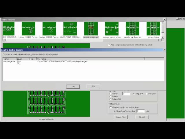
ProntoGERBER-CONNECTION software is used by electronic manufacturer & imports raw Gerber data & allows the user to add intelligent information to the shapes on the display and creates real reference designators, theta rotation, part numbers, X/Y comp

The PCB Footprint Expert is a powerful CAD library development tool powered by our own proprietary CAD LEAP Technology (Libraries Enhanced with Automated Preferences). It is packed with very powerful advanced library management features that cuts foo
Training Courses | | | IPC-600 Specialist (CIS)
The Certified IPC-600 Specialist (CIS) training targets quality assurance and acceptance of bare printed circuit boards.
Events Calendar | Wed Mar 18 00:00:00 EDT 2020 - Wed Mar 18 00:00:00 EDT 2020 | College Park, Maryland USA
CALCE Reliability Science Symposium - Spring 2020
Career Center | Erode, Tamilnadu India | Engineering
Professional Summary 3+ years of experience in the PCB CAM engineering Exposure to FRONTLINE GENESIS 2000 Having exposure in UCAM Exposure to Create, Array & Panelize it for manufacturability Experienced in Creating impedance cou
Career Center | Shen Zhen, China | Management,Sales/Marketing
Working in GLORYPCB for 10 years.knowing electronic supply chain very well. especially for PCB PCBA assembly and other Electronic Manufacturing Service.Glorypcb is a professional electronic manufacturer located in Shenzhen with three facilities.offe
PCB Libraries, Inc. | https://www.pcblibraries.com/forum/RSS_pcb-design-in-the-1970s_topic2333.xml
;The pad master was over-exposed to create the solder mask swell. The PCB’swhere created using the negatives to apply a temporary mask that protects partsof the copper laminate from acid and leaves the desired pattern
| https://www.eptac.com/ask/bubbles-in-conformal-coating/
: If there is a bubble in the conformal coating that covers two traces, but both traces are covered with soldermask is this rejectable


