Industry Directory | Manufacturer
CVInc services advanced packaging. Placing solder bumps on single die, partial wafers, and complete wafers...we also offer RDL (redistribution) services in 5-7 working days. Our custom preforms are as small as 50um geometries.
STATS ChipPAC is a leading provider of advanced semiconductor packaging and test services to global customers in the communication, consumer and computing markets.
This module adds creation of thick-film, thin-film, laminate and ceramic MCMs. Dies are easily captured from any type of data (faxed, standard data files or GDSII). Bonding pads made with any number of rows, straight or curved, fanouts using equal
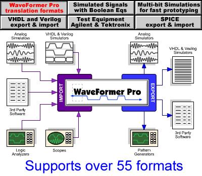
WaveFormer Pro is a revolutionary new rapid-prototyping EDA tool that helps you design faster and with fewer mistakes. WaveFormer Pro enables you to automatically determine critical paths, verify timing margins, adjust for reconvergent fanout effects
Electronics Forum | Wed Nov 23 19:50:23 EST 2016 | gmscribe
Hi guys, I'm working on a design involving a 223-pin BGA with 0.5mm pitch (ball size 0.3mm) with a 16-bit DDR3 controller involved. Currently routing a track between two balls is resulting in a track width of 0.1mm and a spacing of 0.077mm. Now the
Electronics Forum | Fri Nov 25 20:47:54 EST 2016 | sarason
You are coming up against the no of tracks vs density problem. There are basically 2 solutions, more layers so you can get 1 track between each pin as it exits the structure from underneath the IC, say 3 rows of BGA is 2 layers, 5 rows is 4 layers et
Industry News | 2017-08-29 15:41:30.0
The SMTA and Chip Scale Review are pleased to announce the Workshops for the 14th Annual International Wafer-Level Packaging Conference (IWLPC) held October 26th. IWLPC will be held October 24-26, 2017 at the DoubleTree Airport Hotel in San Jose, California.
Industry News | 2016-06-19 19:44:55.0
The SMTA and Chip Scale Review magazine are pleased to announce the Keynote Presenters for the 13th Annual International Wafer-Level Packaging Conference. The IWLPC will be held October 18-20, 2016 at the DoubleTree Airport Hotel in San Jose, California.
Technical Library | 2015-02-05 23:23:40.0
Ball grid arrays are the boon and bane of engineers and printed circuit board designers the world over. Their unparalleled pin density and low lead inductance are essential in today's high pin count, high frequency integrated circuits. However, that same pin density and unique interface create a challenge unique unto themselves. These challenges need to be faced head on since the ball grid array (BGA) is prevalent in modern PCBs. While there are entire textbooks that cover the topic of BGAs, their use and fanout techniques, the quick overview provided here offers an engineer a good starting point for improving BGA designs.
Technical Library | 2021-06-21 19:34:02.0
In this era of electronics miniaturization, high yield and low-cost integrated circuit (IC) substrates play a crucial role by providing a reliable method of high density interconnection of chip to board. In order to maximize substrate real-estate, the distance between Cu traces also known as line and space (L/S) should be minimized. Typical PCB technology consists of L/S larger than 40 µ whereas more advanced wafer level technology currently sits at or around 2 µm L/S. In the past decade, the chip size has decreased significantly along with the L/S on the substrate. The decreasing chip scales and smaller L/S distances has created unique challenges for both printed circuit board (PCB) industry and the semiconductor industry. Fan-out panel-level packaging (FOPLP) is a new manufacturing technology that seeks to bring the PCB world and IC/semiconductor world even closer. While FOPLP is still an emerging technology, the amount of high-volume production in this market space provide a financial incentive to develop innovative solutions in order to enable its ramp up. The most important performance aspect of the fine line plating in this market space is plating uniformity or planarity. Plating uniformity, trace/via top planarity, which measures how flat the top of the traces and vias are a few major features. This is especially important in multilayer processing, as nonuniformity on a lower layer can be transferred to successive layers, disrupting the device design with catastrophic consequences such as short circuits. Additionally, a non-planar surface could also result in signal transmission loss by distortion of the connecting points, like vias and traces. Therefore, plating solutions that provide a uniform, planar profile without any special post treatment are quite desirable.
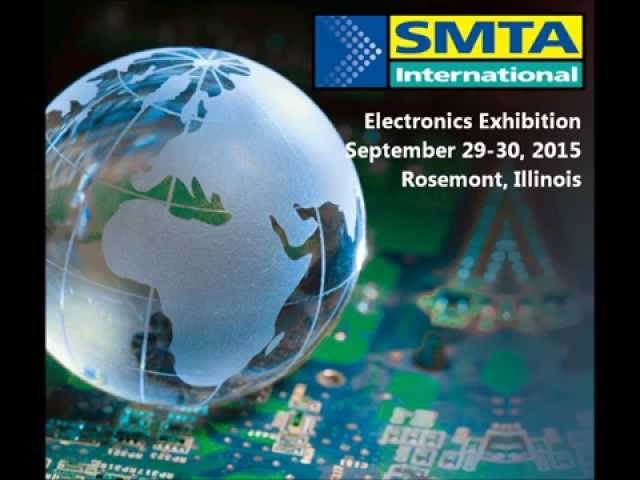
SMTA International Electronics Exhibition Tuesday, September 29: 9am-5pm Wednesday, September 30: 9am-4pm Donald Stephens Convention Center Rosemont, IL See More Equipment & Technology Than Ever Before! Many of the 160 exhibiting companies will bri
Training Courses | | | PCB Design Courses
The PCB design courses teach students the process, techniques and tools needed to design layout of printed circuit boards.
Events Calendar | Sun Sep 27 00:00:00 EDT 2020 - Thu Oct 01 00:00:00 EDT 2020 | Rosemont, Illinois USA
SMTA International 2020 Conference & Exhibition
Events Calendar | Wed Jul 26 00:00:00 EDT 2017 - Wed Jul 26 00:00:00 EDT 2017 | Chicago, Illinois USA
IPC Technical Education - Best Practices in Design
| https://www.eptac.com/wp-content/uploads/eptac/datasheets/EPTAC_DataSheet_PCED.pdf
• Routing for DFX, SI/PI and Layout Solvability • Routing Fanout with HDI, Spacing and Pitch • Routing Power Distribution • General Routing Considerations


