Industry Directory | Distributor / Manufacturer / Manufacturer's Representative / Standards Setting / Certification / Training Provider
PB Technik supplies SMT equipment and materials to the Polish market. JUKI ERSA EKRA BRADY MARANTZ
New Equipment | Rework & Repair Equipment
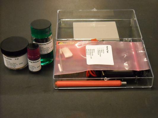
The BEST Gold Contact Replating Kit includes the tools you need for fast replating and modification of circuit contacts. Edge contacts may require replating if they are contaminated with solder or become scratched during handling or do not meet the m
New Equipment | Surface Finish
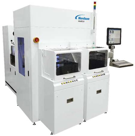
Designed for wafer processing, Nordson MARCH's SPHERE™ series plasma systems, the StratoSPHERE offers superior plasma treatment for high-throughput advanced semiconductor packaging applications. The StratoSPHERE plasma system is ideal for wafer pro
Electronics Forum | Fri Oct 05 18:59:53 EDT 2001 | Dan Steffler
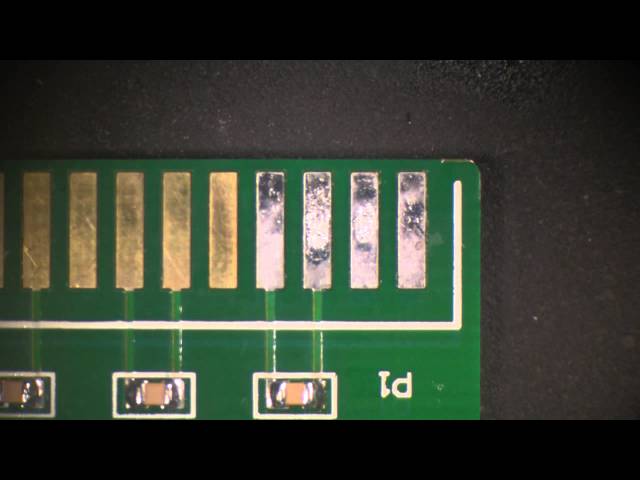
I have had an issue where solder has contaminated gold plated pads (fingers) where it is not acceptable. The pads must remain perfectly coplaniar for a LCD zebra strip to lay accross them. Does anyone know of a way to remove the marriage level of s
Electronics Forum | Wed Jun 13 06:42:14 EDT 2012 | brettrenishaw
We have a problem with our Unleaded wave solder machine only randomly soldering some pads. I have looked at the flux level and that appears fine aswell as cheking the preheat and solder height in the bath. The probelm is not exclusive to one perticul
Industry News | 2013-10-28 16:31:54.0
IPC Conference on Solder and Reliability: Materials, Processes and Tests, November 13–14 in Costa Mesa, Calif.
Industry News | 2018-12-08 03:29:29.0
SMT Dictionary – Surface Mount Technology Acronym and Abbreviation
.jpg)
Parts & Supplies | Pick and Place/Feeders
CYBEROPTICS laser/CYBEROPTICS camera:JUKI laser(570/620/730/740/750/760/2010/2020/2030/2040/2050/2060/2070/2080/KJ-01/KJ-02//FX-1/FX-2/FX-3/3020R/JX-100 laser unit),YAMAHA laser,SAMSUNG laser,TENRYU laser,PHILIPS(ASSEMBLEON) FCM PPU laser,Autotronik
1.jpg)
Parts & Supplies | Pick and Place/Feeders
CYBEROPTICS laser/CYBEROPTICS camera:JUKI laser(570/620/730/740/750/760/2010/2020/2030/2040/2050/2060/2070/2080/KJ-01/KJ-02//FX-1/FX-2/FX-3/3020R/JX-100 laser unit),YAMAHA laser,SAMSUNG laser,TENRYU laser,PHILIPS(ASSEMBLEON) FCM PPU laser,Autotronik
Technical Library | 2020-08-27 01:22:45.0
Initially adopted internal specifications for acceptance of printed circuit boards (PCBs) used for wire bonding was that there were no nodules or scratches allowed on the wirebond pads when inspected under 20X magnification. The nodules and scratches were not defined by measurable dimensions and were considered to be unacceptable if there was any sign of a visual blemish on wire-bondable features. Analysis of the yield at a PCB manufacturer monitored monthly for over two years indicated that the target yield could not be achieved, and the main reasons for yield loss were due to nodules and scratches on the wirebonding pads. The PCB manufacturer attempted to eliminate nodules and scratches. First, a light-scrubbing step was added after electroless copper plating to remove any co-deposited fine particles that acted as a seed for nodules at the time of copper plating. Then, the electrolytic copper plating tank was emptied, fully cleaned, and filtered to eliminate the possibility of co-deposited particles in the electroplating process. Both actions greatly reduced the density of the nodules but did not fully eliminate them. Even though there was only one nodule on any wire-bonding pad, the board was still considered a reject. To reduce scratches on wirebonding pads, the PCB manufacturer utilized foam trays after routing the boards so that they did not make direct contact with other boards. This action significantly reduced the scratches on wire-bonding pads, even though some isolated scratches still appeared from time to time, which caused the boards to be rejected. Even with these significant improvements, the target yield remained unachievable. Another approach was then taken to consider if wire bonding could be successfully performed over nodules and scratches and if there was a dimensional threshold where wire bonding could be successful. A gold ball bonding process called either stand-off-stitch bonding (SSB) or ball-stitch-on-ball bonding (BSOB) was used to determine the effects of nodules and scratches on wire bonds. The dimension of nodules, including height, and the size of scratches, including width, were measured before wire bonding. Wire bonding was then performed directly on various sizes of nodules and scratches on the bonding pad, and the evaluation of wire bonds was conducted using wire pull tests before and after reliability testing. Based on the results of the wire-bonding evaluation, the internal specification for nodules and scratches for wirebondable PCBs was modified to allow nodules and scratches with a certain height and a width limitation compared to initially adopted internal specifications of no nodules and no scratches. Such an approach resulted in improved yield at the PCB manufacturer.
BEST Inc master instructor Norman Mier demonstrates how to replate gold fingers using the BEST gold contact replating kit. In this video he demonstrates how to repair, prepare and replate the finger using a gold replating solution. If you want to lea
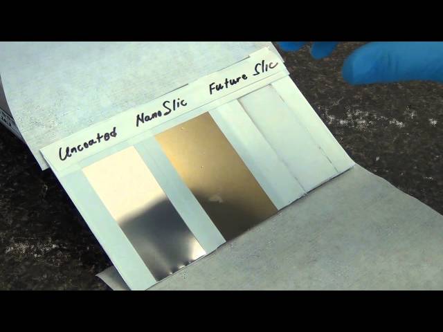
NanoSlic™ Gold is our top of the line spray on coating applied to our UltraSlic™ solder paste stencil, which gives previously unseen performance benefits in transfer efficiency. The NanoSlic™ Gold coating also gives the benefits of improved under-ste
Events Calendar | Tue Jan 23 00:00:00 EST 2018 - Tue Jan 23 00:00:00 EST 2018 | New Milford, Connecticut USA
FREE Webinar: Eliminate Circuit Board Problems and Failure Modes
Career Center | Shen Zhen, China | Management,Sales/Marketing
Working in GLORYPCB for 10 years.knowing electronic supply chain very well. especially for PCB PCBA assembly and other Electronic Manufacturing Service.Glorypcb is a professional electronic manufacturer located in Shenzhen with three facilities.offe
ASYMTEK Products | Nordson Electronics Solutions | https://www.nordson.com/en/industries/medical-life-science-and-pharmaceutical?con=t&page=22
… Fundamentally New Filtration System for Highly Contaminated Plastics Boosts Recycling Productivity and Minimized Melt Loss Polymer Processing Systems Automatic Self-Cleaning BKG® HiCon™
Imagineering, Inc. | https://www.pcbnet.com/blog/understanding-the-pcb-fabrication-process-from-design-to-delivery/
. Physical design rules relating to trace width, differential pairings, pads, and vias. Spacing design rules address the clearance and spacing between components

.gif)
.gif)

