
Industry Directory | Equipment Dealer / Broker / Auctions
Our Company handle AOI (Auto Optical Inspection) and SPI (Solder Paste Inspection) Machines.
Industry Directory | Manufacturer
We are a PCB manufacturer located in China and right now we have set up our office in Ontario, Canada. We can produce high-quality PCBs up to 24 layers and we accept orders for prototypes as well as large volumes, both with very competitive prices.

http://www.flason-smt.com/product/Siemens-12mm-16mm-original-feeder-00141092.html Siemens 12mm 16mm original feeder 00141092 SMT Spare Parts Seimens feeder Siemens 12mm 16mm original feeder 00141092 Usage: Seimens pick and place machine Produ
New Equipment | Rework & Repair Equipment
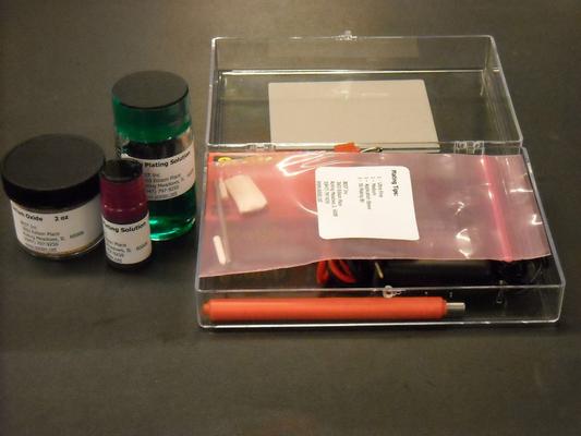
The BEST Gold Contact Replating Kit includes the tools you need for fast replating and modification of circuit contacts. Edge contacts may require replating if they are contaminated with solder or become scratched during handling or do not meet the m
Electronics Forum | Tue Jul 18 03:04:46 EDT 2006 | sharifudin
We are trying to reduce the number of unit fail at QA Visual Inspection due to Solder On Gold Finger. We know so far that the solder is spattering onto the Gold Finger during reflow. I need some advise on what kind of process can improve to reduce th
Electronics Forum | Fri Apr 13 12:37:35 EDT 2001 | edylc
>>> gold finger was covered by a Kapton tape and it was done offline away from the Screen printer or rather from the SMT lines itself, we are using an ENIG Pcb's , the process doesnt need a wave soldering ....however at the final end of the line ,
Used SMT Equipment | In-Circuit Testers
Lot Number: 200 Description: Spea 4060s2 Flying Probe Tester; 2019; S/N TMT267EF; (4) Top-side Probes, (2) Bottom-side Probes; Options: Automatic Optical Inspection - Alignment, Rotation, Presence, Optical Character Verify; 2-Axes & 3-Axes Led Color
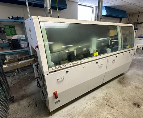
Used SMT Equipment | Soldering - Wave
Speedline Technologies Electrovert EPK Gold Wave Solder Machine - just removered from production in working conditon. Currently in production and available now. 11/2005 DOM, 208VAC 3 Phase Power, Reciprocating Spray Fluxer, L to R Board Flow, Heavy D
Industry News | 2018-10-18 09:06:41.0
Gold Fingers: A Guide to Understanding Gold-Plated PCB Connectors
Industry News | 2019-03-14 11:28:14.0
Precision PCB Services, Inc. Opens New Texas Location

Technical Library | 2020-08-27 01:22:45.0
Initially adopted internal specifications for acceptance of printed circuit boards (PCBs) used for wire bonding was that there were no nodules or scratches allowed on the wirebond pads when inspected under 20X magnification. The nodules and scratches were not defined by measurable dimensions and were considered to be unacceptable if there was any sign of a visual blemish on wire-bondable features. Analysis of the yield at a PCB manufacturer monitored monthly for over two years indicated that the target yield could not be achieved, and the main reasons for yield loss were due to nodules and scratches on the wirebonding pads. The PCB manufacturer attempted to eliminate nodules and scratches. First, a light-scrubbing step was added after electroless copper plating to remove any co-deposited fine particles that acted as a seed for nodules at the time of copper plating. Then, the electrolytic copper plating tank was emptied, fully cleaned, and filtered to eliminate the possibility of co-deposited particles in the electroplating process. Both actions greatly reduced the density of the nodules but did not fully eliminate them. Even though there was only one nodule on any wire-bonding pad, the board was still considered a reject. To reduce scratches on wirebonding pads, the PCB manufacturer utilized foam trays after routing the boards so that they did not make direct contact with other boards. This action significantly reduced the scratches on wire-bonding pads, even though some isolated scratches still appeared from time to time, which caused the boards to be rejected. Even with these significant improvements, the target yield remained unachievable. Another approach was then taken to consider if wire bonding could be successfully performed over nodules and scratches and if there was a dimensional threshold where wire bonding could be successful. A gold ball bonding process called either stand-off-stitch bonding (SSB) or ball-stitch-on-ball bonding (BSOB) was used to determine the effects of nodules and scratches on wire bonds. The dimension of nodules, including height, and the size of scratches, including width, were measured before wire bonding. Wire bonding was then performed directly on various sizes of nodules and scratches on the bonding pad, and the evaluation of wire bonds was conducted using wire pull tests before and after reliability testing. Based on the results of the wire-bonding evaluation, the internal specification for nodules and scratches for wirebondable PCBs was modified to allow nodules and scratches with a certain height and a width limitation compared to initially adopted internal specifications of no nodules and no scratches. Such an approach resulted in improved yield at the PCB manufacturer.
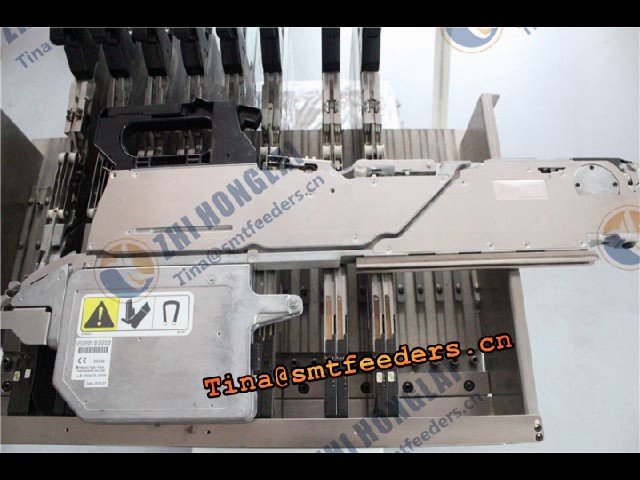
we have many universal gold plus feeders to sell . www.smt-store.com
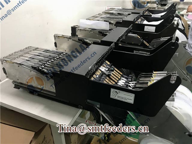
we have many hitachi equipment and hitachi feeders to sell . if you want to know more , please contact us tina@smtfeeders.cn
Training Courses | | | Cable and Wire Harness Assembly Training Courses
Browse training and certification programs for wire harness cable and connector assembly.
Events Calendar | Mon Nov 25 00:00:00 EST 2019 - Mon Nov 25 00:00:00 EST 2019 | ,
Webinar: Overcoming Challenging X-Ray Problems
Career Center | Palmdale, California USA | Quality Control
Plans and conducts activities concerned with the quality control and quality assurance of industrial processes, materials, and products by performing the following duties. Develops and initiates standards and methods for inspection, testing, and eva
Career Center | Milpitas, California USA | Engineering,Production,Quality Control,Research and Development,Technical Support
Winslow Automation, Inc. (aka Six Sigma), an industry leader in electronic component interconnect technology & related test and failure analysis services, is seeking individuals specializing in materials lab testing to join our team. We have openin
Career Center | Shen Zhen, China | Management,Sales/Marketing
Working in GLORYPCB for 10 years.knowing electronic supply chain very well. especially for PCB PCBA assembly and other Electronic Manufacturing Service.Glorypcb is a professional electronic manufacturer located in Shenzhen with three facilities.offe
Career Center | Erode, Tamilnadu India | Engineering
Professional Summary 3+ years of experience in the PCB CAM engineering Exposure to FRONTLINE GENESIS 2000 Having exposure in UCAM Exposure to Create, Array & Panelize it for manufacturability Experienced in Creating impedance cou
Lewis & Clark | https://www.lewis-clark.com/product-tag/gold/
Gold Archives - Lewis and Clark, Inc. Skip to content My Cart: $ 0.00 0 View Cart Checkout No products in the cart. Subtotal: $ 0.00 View Cart Checkout Lewis and Clark, Inc
| https://www.eptac.com/ask/gold-wire-bond-failing-pull-test/
Gold Wire Bond Failing Pull Test - EPTAC - Train. Work Smarter. Succeed Looking for solder training standards, manuals, kits, and more
Our Company handle AOI (Auto Optical Inspection) and SPI (Solder Paste Inspection) Machines.
Equipment Dealer / Broker / Auctions
Hwaseong-si, Gyeonggi-do, Korea
Hwaseong-si, South Korea
Phone: +82-1029254936


