Industry Directory | Manufacturer
Professional, Reliable,High Quality,Low Cost, Rapid Delivery PCB manufacturer
Industry Directory | Manufacturer
Engaged in OEM manufacture Rigid PCB(1-22layer, MCPCB,HDI PCB etc),PCBA,Flex PCB,Rigid-Flex PCB.
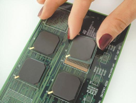
New Equipment | Solder Paste Stencils
Eliminate hours of solder mask damage repair time for bga sites while improving rework yield. Are you frustrated by the time it takes to repair mask damage underneath the BGA during the rework process? Are you squeezed for space on the PCB in an

New Equipment | Wave Soldering
DIP Insertion Line wave soldering machine N250 DIP Insertion Line wave soldering machine DIP Line wave soldering machine DIP wave soldering machine Insertion Line wave soldering machine Weight: 700KG Dimensions: 2600(L)*1200(W)*1600(H)
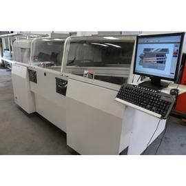
Used SMT Equipment | Soldering - Wave
Lead free wave solder Manufacturing date: 02/10 Volt: 380-3 Made in USA Internal Spray Fluxer 1 Top Pre-Heater 3 Bottom Pre-Heater Nitrogen Option: No Wave Types: Chip and Lambda Conveyor w/fingers: V and L types Preheaters: Conve
Industry News | 2018-10-18 09:06:41.0
Gold Fingers: A Guide to Understanding Gold-Plated PCB Connectors
Industry News | 2014-03-25 09:35:06.0
Count On Tools Inc. (COT)announces the release of the new support plates for its line of ezLOAD Board Supports.
Technical Library | 2021-07-06 21:20:38.0
The evolution of internet-enabled mobile devices has driven innovation in the manufacturing and design of technology capable of high-frequency electronic signal transfer. Among the primary factors affecting the integrity of high-frequency signals is the surface finish applied on PCB copper pads – a need commonly met through the electroless nickel immersion gold process, ENIG. However, there are well-documented limitations of ENIG due to the presence of nickel, the properties of which result in an overall reduced performance in high-frequency data transfer rate for ENIG-applied electronics, compared to bare copper.
Technical Library | 2020-08-27 01:22:45.0
Initially adopted internal specifications for acceptance of printed circuit boards (PCBs) used for wire bonding was that there were no nodules or scratches allowed on the wirebond pads when inspected under 20X magnification. The nodules and scratches were not defined by measurable dimensions and were considered to be unacceptable if there was any sign of a visual blemish on wire-bondable features. Analysis of the yield at a PCB manufacturer monitored monthly for over two years indicated that the target yield could not be achieved, and the main reasons for yield loss were due to nodules and scratches on the wirebonding pads. The PCB manufacturer attempted to eliminate nodules and scratches. First, a light-scrubbing step was added after electroless copper plating to remove any co-deposited fine particles that acted as a seed for nodules at the time of copper plating. Then, the electrolytic copper plating tank was emptied, fully cleaned, and filtered to eliminate the possibility of co-deposited particles in the electroplating process. Both actions greatly reduced the density of the nodules but did not fully eliminate them. Even though there was only one nodule on any wire-bonding pad, the board was still considered a reject. To reduce scratches on wirebonding pads, the PCB manufacturer utilized foam trays after routing the boards so that they did not make direct contact with other boards. This action significantly reduced the scratches on wire-bonding pads, even though some isolated scratches still appeared from time to time, which caused the boards to be rejected. Even with these significant improvements, the target yield remained unachievable. Another approach was then taken to consider if wire bonding could be successfully performed over nodules and scratches and if there was a dimensional threshold where wire bonding could be successful. A gold ball bonding process called either stand-off-stitch bonding (SSB) or ball-stitch-on-ball bonding (BSOB) was used to determine the effects of nodules and scratches on wire bonds. The dimension of nodules, including height, and the size of scratches, including width, were measured before wire bonding. Wire bonding was then performed directly on various sizes of nodules and scratches on the bonding pad, and the evaluation of wire bonds was conducted using wire pull tests before and after reliability testing. Based on the results of the wire-bonding evaluation, the internal specification for nodules and scratches for wirebondable PCBs was modified to allow nodules and scratches with a certain height and a width limitation compared to initially adopted internal specifications of no nodules and no scratches. Such an approach resulted in improved yield at the PCB manufacturer.

StencilQuik demonstration video. This breakthrough method allows you to simplify placement/replacement saving 50% or more of time required to rework BGAs or CSPs.This is a well developed BGA rework method. More on the StencilQuik(TM) process here:

www.unisoft-cim.com/pcbplace.htm - The ProntoPLACE module from Unisoft is used by electronics manufacturers to generate the necessary programs for automatic PCB assembly machines in minutes. ProntoPLACE programs most popular surface mount (SMT) place
Events Calendar | Tue Apr 19 18:30:00 UTC 2022 - Tue Apr 19 18:30:00 UTC 2022 | ,
Virtual Course: Selection Criteria of Surface Finish for Next Generation PCB Technologies
Career Center | North San Jose, California USA | Engineering
My client, one of the leading Electronics Manufacturing Services (EMS) companies in the world has an urgent need for Optical Engineers in the Bay Area. They are looking for Process, Test, Component Engineers as well as Optical Technicians. These ne
Career Center | Frederick, Maryland USA | Production,Technical Support
MUST BE WILLING TO BECOME FULLY VACCINATED FOR COVID-19, OR QUALIFY FOR A RECOGNIZED EXEMPTION, TO WORK AT ACDI IF GOVERNMENT CONTRACTOR REGULATIONS ARE UPHELD. OUR COMPANY What we do day-in and day-out has a lasting, meaningful impact across man
Career Center | Erode, Tamilnadu India | Engineering
Professional Summary 3+ years of experience in the PCB CAM engineering Exposure to FRONTLINE GENESIS 2000 Having exposure in UCAM Exposure to Create, Array & Panelize it for manufacturability Experienced in Creating impedance cou
Career Center | Stoneham, | Engineering,Production,Research and Development,Technical Support
Warren P. Pumyea 8 Beacon Street Stoneham, Massachusetts 02180 Cell #: 978-821-7335 * E-mail: warren@pumyea.com http://www.pumyea.com/Process_Manufacturing_Engineer.doc Objective: Seeking a position as an engineer or related discipline whic
PCB Libraries, Inc. | https://www.pcblibraries.com/forum/ipc-standards-for-manufacturing-assembly_topic877_post9030.html
IPC Standards for Manufacturing & Assembly - PCB Libraries Forum Forum Home > PCB Library Expert > Questions & Answers New Posts FAQ Search Events Register Login IPC Standards for Manufacturing
| https://unisoft-cim.com/cells-apparel.php
PCB Product and Job Tracking Manufacturing Execution System MES Software | Unisoft ≡ Menu Skip navigation For over 35 years, Intelligent PCB Manufacturing Automation Software Be production ready in minutes, not days


