
http://www.flason-smt.com/product/Siemens-12mm-16mm-original-feeder-00141092.html Siemens 12mm 16mm original feeder 00141092 SMT Spare Parts Seimens feeder Siemens 12mm 16mm original feeder 00141092 Usage: Seimens pick and place machine Produ
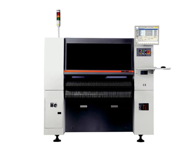
Hanwha SM482 Plus Pick and Place Machine Speed : 30,000CPH (Optimum) PCB : Max. 460(L) x400(W) Structure : 1 Gantry x 6 Spindles/Head Component range: 0402 ~ 55mm(H 15mm) Product description: Hanwha SM482 Plus Pick and Place Machine, Speed : 3
Electronics Forum | Fri Jul 08 06:38:51 EDT 2005 | mattkehoe
I did not get that info. We sent them back and the vendor ran them through HASL finish. They processed very well after that. Thanks to everyone for the help. mk
Electronics Forum | Fri Apr 09 15:00:04 EDT 2010 | davef
So for your SMT1/SMT2/PTH boards, you have poor solderability during SMT2. [Even if you have no SMT2 and only ST1/PTH, our answer is the same.] We assume this occurs on one board part number only. We guess that your bare boards have insufficient gol
Industry News | 2018-10-18 11:08:03.0
Different Techniques for Plating
Industry News | 2018-12-08 03:38:44.0
Lead-Free (Pb-Free) Solder and Composition
Technical Library | 2020-08-05 18:49:32.0
The evolution of internet-enabled mobile devices has driven innovation in the manufacturing and design of technology capable of high-frequency electronic signal transfer. Among the primary factors affecting the integrity of high-frequency signals is the surface finish applied on PCB copper pads – a need commonly met through the electroless nickel immersion gold process, ENIG. However, there are well-documented limitations of ENIG due to the presence of nickel, the properties of which result in an overall reduced performance in high-frequency data transfer rate for ENIG-applied electronics, compared to bare copper. An innovation over traditional ENIG is a nickel-less approach involving a special nano-engineered barrier designed to coat copper contacts, finished with an outermost gold layer. In this paper, assemblies involving this nickel-less novel surface finish have been subjected to extended thermal exposure, then intermetallics analyses, contact/sheet resistance comparison after every reflow cycle (up to 6 reflow cycles) to assess the prevention of copper atoms diffusion into gold layer, solder ball pull and shear tests to evaluate the aging and long-term reliability of solder joints, and insertion loss testing to gauge whether this surface finish can be used for high-frequency, high density interconnect (HDI) applications.
SMTnet Express, September 7, 2017, Subscribers: 30,782, Members: Companies: 10,712, Users: 23,761 Challenges on ENEPIG Finished PCBs: Gold Ball Bonding and Pad Metal Lift Young K. Song and Vanja Bukva; Teledyne DALSA As a surface finish for PCBs
SMTnet Express, August 7, 2014, Subscribers: 23058, Members: Companies: 13975, Users: 36604 Gold Embrittlement In Lead-Free Solder. Craig Hillman, Nathan Blattau, Joelle Arnold, Thomas Johnston, Stephanie Gulbrandsen; DfR Solutions , Julie Silk
Heller Industries Inc. | https://hellerindustries.com/wp-content/uploads/2022/04/Vacuum-Void-Reduction-Reflow-1.pdf
. Half of the population of test vehicles then were re-processed (reflowed) using vacuum reflow. Transmission x-ray inspection showed a significant reduction in solder voiding after vacuum processing
Heller 公司 | http://hellerindustries.com.cn/Vacuum-Void-Reduction-Reflow.pdf
. Half of the population of test vehicles then were re-processed (reflowed) using vacuum reflow. Transmission x-ray inspection showed a significant reduction in solder voiding after vacuum processing


