Advance Devices, Inc. offers Smart Tweezers LCR Meter - excellent tool for identification testing of SMD Components.
Industry Directory | Consultant / Service Provider / Manufacturer
Delkin Devices, Inc. is an independently owned business and the largest US memory card manufacturer in San Diego, CA.
New Equipment | Cleaning Equipment
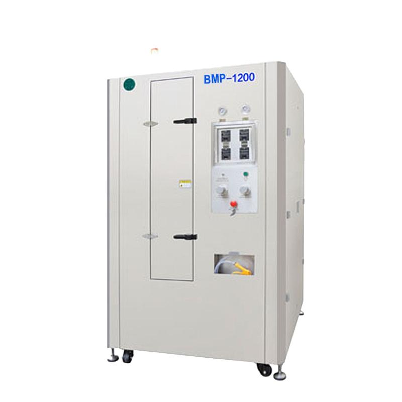
Automatick Ultrasonic Stencil Cleaner BMP-1200 ▶All stainless steel body: beautiful, wear resistance, corrosion resistance, acid, alkaline and other cleaning fluid. Meet environmental protection requirements and standards. ▶Full pneumatic operation,
New Equipment | Cleaning Equipment
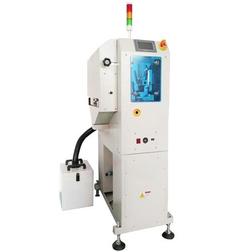
PCB Surface Cleaning Machine SMM-450 PCB Surface Cleaning Machine SMM-450 The PCB Cleaning Machine is used to remove filth on the surface of PCB. Technical Parameters 1. Independent innovation patent design (patent: 2017SR471774), the industry's
Electronics Forum | Thu Aug 21 17:17:47 EDT 2003 | justin
Do some push / pull testing. Typically with black pad, you can flick the components right off the board. If you have this, the boards are about as reliable as a Yugo. If you get decent push / pull results, odds are you don't have black pad and you
Electronics Forum | Tue Apr 26 11:22:48 EDT 2005 | denismeloche
I have found that Sn62 solder gives better strength and leach resistance when soldering to gold surfaces. The gold needs to be at least 5 to 10 micro inches thick to prevent nickel oxidation but if over 25 micro inches will cause brittleness. I hav

Used SMT Equipment | Soldering - Wave
Senju Lead Free Wave SPF-300 Very Nice clean machine Dual Wave Solder No Nitrogen No Top Preheat Zones 355mm Max PCB width 3x Bottom Radiant Preheat Zones SPF-300

Used SMT Equipment | Screen Printers
DEK 03IX automatic solder paste printing machine features advanced up/down k-view vision system, independent control and adjustment of lighting, high-speed moving lens, accurate alignment of PCB PCB and net board. The DEK Horizon 03IX automatic solde
Industry News | 2018-12-08 03:29:29.0
SMT Dictionary – Surface Mount Technology Acronym and Abbreviation
Industry News | 2013-02-20 18:54:10.0
IPC — Association Connecting Electronics Industries® presented Committee Leadership, Distinguished Committee Service and Special Recognition Awards at IPC APEX EXPO® at the San Diego Convention Center.
1.jpg)
Parts & Supplies | Screen Printers
DEK 107645 Circuit breakers device Gasket MORE DEK PARTS IN STOCKS DEK STEPPER MOTOR 140452-181245 DEK SPRING SHAFT KIT 145884 DEK SPRING G0332 DEK SOLVENT PUMP ASSY 191088 DEK SOLVENT 183668 DEK SOLENOID VALVE 165431 DEK SINGLE BOARD COMPUT
Parts & Supplies | Assembly Accessories
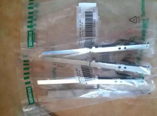
Detailed Product Description Brand: Siemens Country: China Shenzhen Condition: Good Quanlity Model: 00322180S03 Use: For Siemens 12/16mm Feeder Name: Feeder Spring Plate 00322180S03 spring plate complete SMT Spare Parts For Siemens 12/16mm Feeder
Technical Library | 2014-08-07 15:13:44.0
Gold embrittlement in SnPb solder is a well-known failure mechanism in electronic assembly. To avoid this issue, prior studies have indicated a maximum gold content of three weight percent. This study attempts to provide similar guidance for Pb-free (SAC305) solder. Standard surface mount devices were assembled with SnPb and SAC305 solder onto printed boards with various thicknesses of gold plating. The gold plating included electroless nickel immersion gold (ENIG) and electrolytic gold of 15, 25, 35, and 50 microinches over nickel. These gold thicknesses resulted in weight percentages between 0.4 to 7.0 weight percent.
Technical Library | 2020-08-27 01:22:45.0
Initially adopted internal specifications for acceptance of printed circuit boards (PCBs) used for wire bonding was that there were no nodules or scratches allowed on the wirebond pads when inspected under 20X magnification. The nodules and scratches were not defined by measurable dimensions and were considered to be unacceptable if there was any sign of a visual blemish on wire-bondable features. Analysis of the yield at a PCB manufacturer monitored monthly for over two years indicated that the target yield could not be achieved, and the main reasons for yield loss were due to nodules and scratches on the wirebonding pads. The PCB manufacturer attempted to eliminate nodules and scratches. First, a light-scrubbing step was added after electroless copper plating to remove any co-deposited fine particles that acted as a seed for nodules at the time of copper plating. Then, the electrolytic copper plating tank was emptied, fully cleaned, and filtered to eliminate the possibility of co-deposited particles in the electroplating process. Both actions greatly reduced the density of the nodules but did not fully eliminate them. Even though there was only one nodule on any wire-bonding pad, the board was still considered a reject. To reduce scratches on wirebonding pads, the PCB manufacturer utilized foam trays after routing the boards so that they did not make direct contact with other boards. This action significantly reduced the scratches on wire-bonding pads, even though some isolated scratches still appeared from time to time, which caused the boards to be rejected. Even with these significant improvements, the target yield remained unachievable. Another approach was then taken to consider if wire bonding could be successfully performed over nodules and scratches and if there was a dimensional threshold where wire bonding could be successful. A gold ball bonding process called either stand-off-stitch bonding (SSB) or ball-stitch-on-ball bonding (BSOB) was used to determine the effects of nodules and scratches on wire bonds. The dimension of nodules, including height, and the size of scratches, including width, were measured before wire bonding. Wire bonding was then performed directly on various sizes of nodules and scratches on the bonding pad, and the evaluation of wire bonds was conducted using wire pull tests before and after reliability testing. Based on the results of the wire-bonding evaluation, the internal specification for nodules and scratches for wirebondable PCBs was modified to allow nodules and scratches with a certain height and a width limitation compared to initially adopted internal specifications of no nodules and no scratches. Such an approach resulted in improved yield at the PCB manufacturer.

Camera Module Cleaning Machine ETA-C800 If you could not find any similar items you want, you may send some photos to us. because our catalog and website haven't included all of our products. PCBA Cleaning Machine, On-line PCBA Cleaning Machine
PCB Surface Cleaning Machine MLPCM-450 Technical Parameters 1. Independent innovation patent design (patent: 2017SR471774), the industry's first, lets you have the most advanced contact cleaning system in the industry. 2. Using Panasonic PLC program
Career Center | Houston, Texas USA | Engineering,Management,Quality Control,Technical Support
Seasoned Process & Quality Engineer. Degreed Chemical Engineer. 20+ years in Electronics Semiconductor manufacturing. Proficient in Quality Statistical tools, Design of Experiments, FMEAs, APQP, PPAP, ISO 9000, ISO/TS 16949 etc.
Career Center | Shen Zhen, China | Management,Sales/Marketing
Working in GLORYPCB for 10 years.knowing electronic supply chain very well. especially for PCB PCBA assembly and other Electronic Manufacturing Service.Glorypcb is a professional electronic manufacturer located in Shenzhen with three facilities.offe
SMTnet Express, August 7, 2014, Subscribers: 23058, Members: Companies: 13975, Users: 36604 Gold Embrittlement In Lead-Free Solder. Craig Hillman, Nathan Blattau, Joelle Arnold, Thomas Johnston, Stephanie Gulbrandsen; DfR Solutions , Julie Silk
| https://www.eptac.com/soldertips/soldertips-solderability-issues-with-nickle-plated-surfaces/
SolderTips: Solderability Issues with Nickle Plated Surfaces | EPTAC Skip to content Scroll Toll Free: 800.643.7822 Toggle navigation Training All Classes
| https://www.smtfactory.com/What-is-an-LED-Flip-Chip-id3680601.html
. Flip chip can be packaged as Gold-free wire, which reduces the probability of device dead lamp from the source. Fourthly, the size can be smaller, the cost of product maintenance can be reduced, and the optics can be more easily matched


