Industry Directory | Manufacturer's Representative
Specialty materials for SMT Assembly. Solder Paste, Spheres, Tac Fluxes, Flip Chip Fluxes, Solder wi
Industry Directory | Manufacturer
Manufacturer of sintering, electrically conductive materials. Applications include semiconductor die attach, component attach, via fill, z-axis interconnection, conductive lines and traces and plated-through hole fill.

New Equipment | Solder Materials
Solder dross has gone from being a cost to be considered by large companies to a very high cost that must be tracked for all who assemble electronic devices.As much as 70% of bar solder can be wasted as solder dross and with SAC 305 now at the $25/Lb

New Equipment | Solder Materials
Solder dross has gone from being a cost to be considered by large companies to a very high cost that must be tracked for all who assemble electronic devices.As much as 70% of bar solder can be wasted as solder dross and with SAC 305 now at the $25/Lb
Electronics Forum | Mon Mar 30 03:10:44 EST 1998 | Patrick Ng
Hi, We have encountered de-wetting issues with gold plated components( SMT LEDs ). The problem comes and go and we yet to locate the root cause ( process, component or solder paste etc ). The rest of the components on the boards are not having this
Electronics Forum | Mon Mar 30 12:55:16 EST 1998 | Justin Medernach
| Hi, | We have encountered de-wetting issues with gold plated components( SMT LEDs ). | The problem comes and go and we yet to locate the root cause ( process, component or solder paste etc ). | The rest of the components on the boards are not havi
Industry News | 2018-10-18 09:06:41.0
Gold Fingers: A Guide to Understanding Gold-Plated PCB Connectors
Industry News | 2018-10-18 08:21:10.0
How to Prevent Non-Wetting Defect during the SMT Reflow Process

Parts & Supplies | Pick and Place/Feeders
KHY-M221A-A0 KGT-M221A-A0 YAMAHA YG12 tank chain gland KHY-M2267-00 YG12 tank chain YS12 towline keel X axis PISCO SP2550 R75 KHY-M2276-S0 YS12 screw X-axis YG12 X-axis screw YG12F YS12F screw guide KHY-M371R-00 RAIL GUIDE 12P YS24 YS100 Feida pl
Technical Library | 2014-08-07 15:13:44.0
Gold embrittlement in SnPb solder is a well-known failure mechanism in electronic assembly. To avoid this issue, prior studies have indicated a maximum gold content of three weight percent. This study attempts to provide similar guidance for Pb-free (SAC305) solder. Standard surface mount devices were assembled with SnPb and SAC305 solder onto printed boards with various thicknesses of gold plating. The gold plating included electroless nickel immersion gold (ENIG) and electrolytic gold of 15, 25, 35, and 50 microinches over nickel. These gold thicknesses resulted in weight percentages between 0.4 to 7.0 weight percent.
Technical Library | 2023-08-04 15:27:30.0
A designed experiment evaluated the influence of several variables on appearance and strength of Pb-free solder joints. Components, with leads finished with nickel-palladium-gold (NiPdAu), were used from Texas Instruments (TI) and two other integrated circuit suppliers. Pb-free solder paste used was tin-silver-copper (SnAgCu) alloy. Variables were printed wiring board (PWB) pad size/stencil aperture (the pad finish was consistent; electrolysis Ni/immersion Au), reflow atmosphere, reflow temperature, Pd thickness in the NiPdAu finish, and thermal aging. Height of solder wetting to component lead sides was measured for both ceramic plate and PWB soldering. A third response was solder joint strength; a "lead pull" test determined the maximum force needed to pull the component lead from the PWB. This paper presents a statistical analysis of the designed experiment. Reflow atmosphere and pad size/stencil aperture have the greatest contribution to the height of lead side wetting. Reflow temperature, palladium thickness, and preconditioning had very little impact on side-wetting height. For lead pull, variance in the data was relatively small and the factors tested had little impact.

ACI Technologies Inc. (ACI) is a scientific research corporation dedicated to the advancement of electronics manufacturing processes and materials for The Department of Defense and industry. This video provides an overview of our commercial service
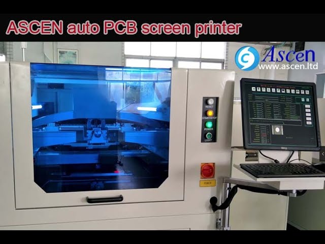
https://www.ascen.ltd/Products/Solder_paste_printer/513.html full auto PCB screen printer and SMT solder paste printing machine with Image and optical system,It is a very accurate fully automatic SMT stencil printer.automatic PCB screen printer main
Training Courses | | | PCB Rework and Hand Soldering Courses
The PCB rework and hand soldering courses courses cover techniques of rework and repair of PCBs, BGAs and other electronics assemblies, and teach fundamentals of soldering of electronics assemblies.
Training Courses | | | IPC-600 Specialist (CIS)
The Certified IPC-600 Specialist (CIS) training targets quality assurance and acceptance of bare printed circuit boards.
Events Calendar | Tue Feb 12 00:00:00 EST 2019 - Tue Feb 12 00:00:00 EST 2019 | ,
Webinar: BGA and Area Array Process Defects - Causes & Cures
Events Calendar | Tue Jan 23 00:00:00 EST 2018 - Tue Jan 23 00:00:00 EST 2018 | New Milford, Connecticut USA
FREE Webinar: Eliminate Circuit Board Problems and Failure Modes
Career Center | Houston, Texas USA | Engineering,Management,Quality Control,Technical Support
Seasoned Process & Quality Engineer. Degreed Chemical Engineer. 20+ years in Electronics Semiconductor manufacturing. Proficient in Quality Statistical tools, Design of Experiments, FMEAs, APQP, PPAP, ISO 9000, ISO/TS 16949 etc.
Career Center | faridabad, India | Engineering,Production,Quality Control
My technical proficiency is extensive and is summarized on my resume (attached). As reflected on my resume (attached) I have completed my B-tech this Year.I am a fresher Electronics Engineer but having 6 months of PCB Assembling,PCB Manufacturing and
SMTnet Express, August 7, 2014, Subscribers: 23058, Members: Companies: 13975, Users: 36604 Gold Embrittlement In Lead-Free Solder. Craig Hillman, Nathan Blattau, Joelle Arnold, Thomas Johnston, Stephanie Gulbrandsen; DfR Solutions , Julie Silk
SMT Express, Issue No. 5 - from SMTnet.com Volume 1, Issue No. 5 Wednesday, October 13, 1999 Featured Article Return to Front Page A New Light-Weight Electronic Packaging Technology Based On Spray-Formed Silicon-Aluminiumby David M. Jacobson
Imagineering, Inc. | https://www.pcbnet.com/blog/how-pcbs-are-made/
: This printed layer contains labels, symbols, and markings for components. Vias: Small holes drilled through the PCB, often plated with copper. Pads
Surface Mount Technology Association (SMTA) | https://www.smta.org/knowledge/journal.cfm
INNOVATIONS FOR ADVANCED MEDICAL ELECTRONIC APPLICATIONS Vern Solberg Abstract 21-2 EFFECTS OF STORAGE ENVIRONMENTS ON THE SOLDERABILITY OF NICKEL-PALLADIUM-GOLD FINISH WITH Pb-BASED AND Pb-FREE SOLDERS Edwin Lopez, Paul Vianco, Samuel Lucero, and Carly


