Industry Directory | Manufacturer
2Layers - 18Layers ;HASL, OSP, Gold plating, immersion Gold/Silver/Tin, removable mask, gold-finger, carbon ink;Conact Person:Rene E-mail:rene@speedingcircuit.com Website:www.speedingcircuit.com
Industry Directory | Manufacturer
Professional, Reliable,High Quality,Low Cost, Rapid Delivery PCB manufacturer
New Equipment | Rework & Repair Services
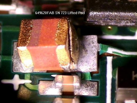
PCB Repair Services BEST is your experienced resource for high value added PCB repair services. If you need any of the following completed to your printed circuit board then let the experts at BEST be your answer: Pad repair services Pad replace
New Equipment | Rework & Repair Equipment
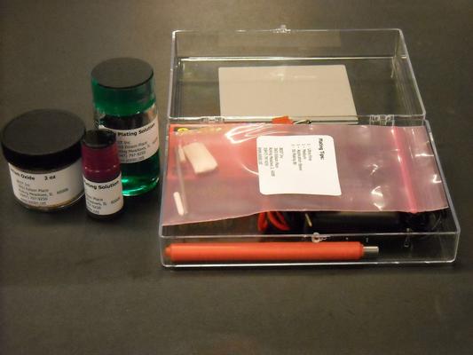
The BEST Gold Contact Replating Kit includes the tools you need for fast replating and modification of circuit contacts. Edge contacts may require replating if they are contaminated with solder or become scratched during handling or do not meet the m
Electronics Forum | Tue Jul 18 22:11:13 EDT 2006 | davef
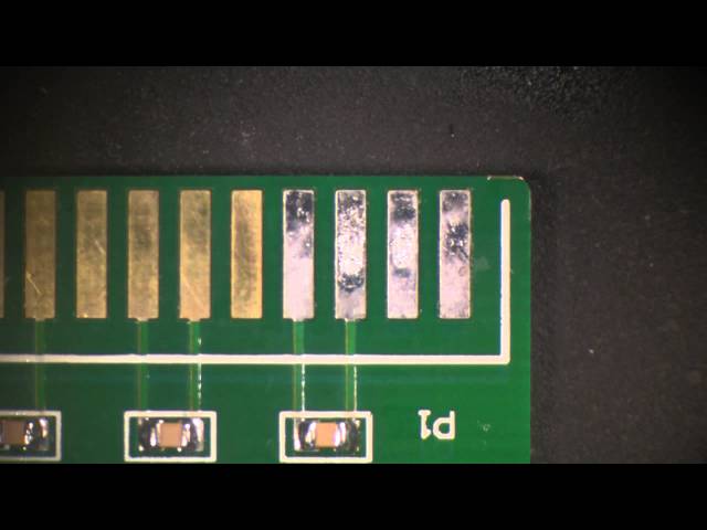
Aping Russ' reply: * ~70% of the time solder on gold fingers is caused by poor printing and handling processes. * ~25% of the time solder on gold fingers is caused by poor thermal recipe when soldering. * ~5% of the time solder on gold fingers is cau
Electronics Forum | Tue Jul 18 10:08:19 EDT 2006 | pms
kapton tape the gold fingers before reflow.........
Industry News | 2018-10-18 09:06:41.0
Gold Fingers: A Guide to Understanding Gold-Plated PCB Connectors
Industry News | 2019-03-14 11:28:14.0
Precision PCB Services, Inc. Opens New Texas Location

Parts & Supplies | Circuit Board Assembly Products
1). FR-4 Material 2). 2 layer, 1.2mm thick 3). 1 oz copper weight. 4). LPI Green solder mask/White silk screen 5). Gold finger 40 microinch, bevelled. 6). HASL + Gold finger, ENIG + gold finger 7). Larg volum, punch contour.

Parts & Supplies | Tape and Reel
High Temperature Masking dots High temperature masking tape and dots are ideal for masking gold fingers of printed circuit boards during wave solder or solder dip process, as well as for solder wave masking and electrical insulation. The p

Safe, precision rework for SMD, BGA, and other high value chips The versatile SV560A rework station combines precision, reliability, and affordability in an all-in-one solution for all your rework needs, from complex, densely populated PCBAs to simpl
BEST Inc master instructor Norman Mier demonstrates how to replate gold fingers using the BEST gold contact replating kit. In this video he demonstrates how to repair, prepare and replate the finger using a gold replating solution. If you want to lea
Career Center | Erode, Tamilnadu India | Engineering
Professional Summary 3+ years of experience in the PCB CAM engineering Exposure to FRONTLINE GENESIS 2000 Having exposure in UCAM Exposure to Create, Array & Panelize it for manufacturability Experienced in Creating impedance cou
Career Center | Shen Zhen, China | Management,Sales/Marketing
Working in GLORYPCB for 10 years.knowing electronic supply chain very well. especially for PCB PCBA assembly and other Electronic Manufacturing Service.Glorypcb is a professional electronic manufacturer located in Shenzhen with three facilities.offe


