Industry Directory | Manufacturer
Reflow ovens for automated SMT PCB assembly, specializing in lead free processing and nitrogen reflow. The best convection reflow ovens on the market.
Industry Directory | Manufacturer / Manufacturer's Representative
We specialize in EMI Ferrite Core, Thermal Pads, Gaskets and shielding products.
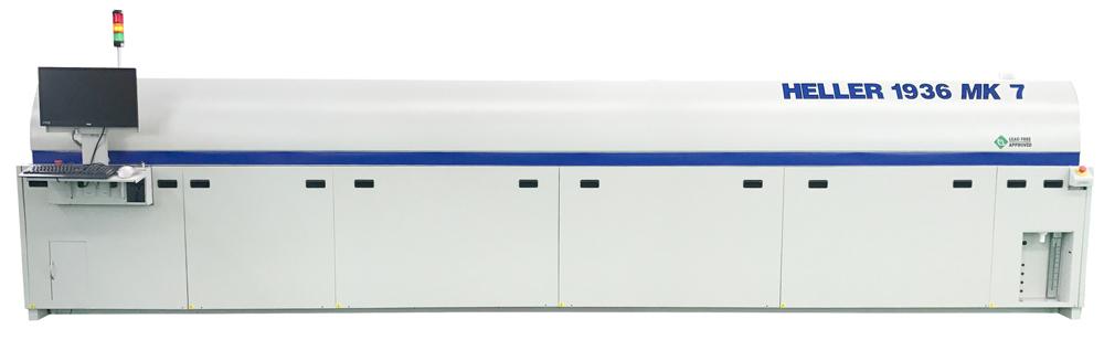
Convection Reflow Oven The World's Best Convection Reflow Oven for High-Throughput The New reflow oven platform revolutionizes the Convection Reflow Oven / Reflow Soldering industry with several new and ground breaking designs! The MK7 convecti
New Equipment | Rework & Repair Services
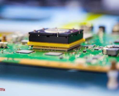
Reliable LGA Rework Services to Rescue Your Project BEST is your source for LGA rework services. We can optimize our processes to make sure voiding is minimized and the interconnection to all of the IO meets the IPC classification for the assembly.

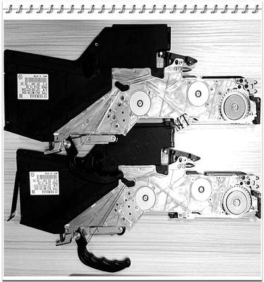
Used SMT Equipment | Repair/Rework
SPLIT VISION MICROSCOPE STEREO WILD M3Z MICROSCOPE WITH ZOOM LENS COLOR DIGITAL CAMERA CAMERA MONITOR REMOTE KEY PAD CONTROLLER AIR/NITRO INLET INCLUDES 3 EACH NOZZLES FOOT SWITCH FOR GAS FLOW TOP AND BOTTOM 800 WATT HEATERS VENTURE VACUUM SYSTEM GRO
Used SMT Equipment | General Purpose Equipment
Blue M Mechanical Convection Oven, 96 cu.ft., F4 Control Product includes the following installed options: Computer Interface: RS485 Standard with Controller Door Style: Standard Double Door Door Hinge: Standard Special ETO Option : Install leve
Industry News | 2018-08-16 19:58:50.0
The SMTA Capital Chapter is holding its upcoming Capital Expo and Tech Forum at Johns Hopkins University / Applied Physics Lab, Kossiakoff Center, 11100 Johns Hopkins Road, Laurel, MD 20723, on Thursday, August 23rd.
Industry News | 2022-10-13 07:44:15.0
I.C.T SMT Vacuum Reflow Oven Machine helps you to solve the problem of High Solder Voids Rates
Technical Library | 2014-09-11 11:36:46.0
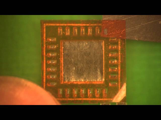
There are a variety of methods one can use to rework QFNs. This paper explains one of the ways to get very little center ground voiding while making it easy to place a tiny component with almost no keep out areas.
Technical Library | 2018-09-26 20:33:26.0
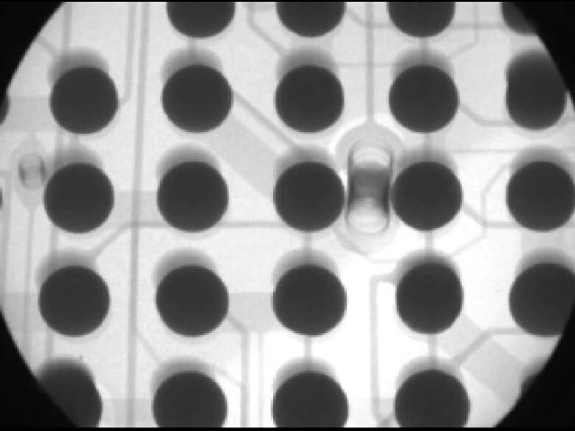
Bottom terminated components, or BTCs, have been rapidly incorporated into PCB designs because of their low cost, small footprint and overall reliability. The combination of leadless terminations with underside ground/thermal pads have presented a multitude of challenges to PCB assemblers, including tilting, poor solder fillet formation, difficult inspection and – most notably – center pad voiding. Voids in large SMT solder joints can be difficult to predict and control due to the variety of input variables that can influence their formation. Solder paste chemistries, PCB final finishes, and reflow profiles and atmospheres have all been scrutinized, and their effects well documented. Additionally, many of the published center pad voiding studies have focused on optimizing center pad footprint and stencil aperture designs. This study focuses on I/O pad stencil modifications rather than center pad modifications. It shows a no-cost, easily implemented I/O design guideline that can be deployed to consistently and repeatedly reduce void formation on BTC-style packages.
Training Courses | | | PCB Rework and Hand Soldering Courses
The PCB rework and hand soldering courses courses cover techniques of rework and repair of PCBs, BGAs and other electronics assemblies, and teach fundamentals of soldering of electronics assemblies.
Training Courses | | | PCB Rework and Hand Soldering Courses
The PCB rework and hand soldering courses courses cover techniques of rework and repair of PCBs, BGAs and other electronics assemblies, and teach fundamentals of soldering of electronics assemblies.
Events Calendar | Tue May 30 18:30:00 UTC 2023 - Tue May 30 18:30:00 UTC 2023 | Holtsville, New York USA
Long Island Chapter Meeting: Fine Feature Paste Printing, Stencil Design and Solder Technology
SMTnet Express, September 27, 2018, Subscribers: 31,354, Companies: 11,055, Users: 25,237 Assessing the Effectiveness of I/O Stencil Aperture Modifications on BTC Void Reduction Carlos Tafoya, Gustavo Ramirez, Timothy O'Neill; AIM Solder Bottom
SMTnet Express, September 14, 2023, Subscribers: 25,056, Companies: 11,888, Users: 28,338 █ Electronics Manufacturing Technical Articles Effects of Assebly Process Variables on Voiding at a Thermal Interface. The present work offers a
PCB Libraries, Inc. | https://www.pcblibraries.com/Forum/bga-pad-size_topic2607_post10645.html
. This was and is expensive. The via-in-pad must be plugged, plated over and planarized flat. Any dimple will trap air and cause Ball Voiding
Heller Industries Inc. | https://hellerindustries.com/wp-content/uploads/2018/07/last-will-of-bga-void.pdf
) resulted in significantly more voids in BGA/CSP solder joints than no Via in Pad design The voiding percentage in area or diameter of the BGA solder joints did not correlate to the failure cycle in thermal cycling (Figure 7) Figure 7. Scatter Chart Showing
.JPG)


