Industry Directory | Manufacturer
Manufacturer of high-speed automated inspection equipment.

Technical specification: I. Hardware System models / types Windows XP Professional Overall FootPrint (LxWxH) 800mm*850mm*1700mm Weight (Approximate) 150KG Adjustable machine
ISIS� (Infrared Screening and Inspection Solutions) was developed to detect defects and manufacturing flaws in printed circuit boards (PCBs) that are assembled using surface mount technology (SMT). ISIS� uses infrared imaging and proprietary thermal
Electronics Forum | Sun Aug 13 22:26:01 EDT 2017 | dawson
Anyone who knows how to prevent such > flaw? > > Tombstones are those lifted components > from one sides. This results in costly and > time-consuming amounts of touch-up and re-work > after the assembly is completed. For the > customers, this e
Electronics Forum | Mon Aug 14 03:25:51 EDT 2017 | spoiltforchoice
There is no solution in above case, this is > caused by the PCB design. There are no > thermals on the pads connected to the copper > poured area. So the other pad reflow first and > lift the component. Yes, this. You could try playing with
.JPG)
Used SMT Equipment | Pick and Place/Feeders
Universal GSM2 Placement Machine With PTF For Sale High Volume, Fine Pitch Placement Design Precision Linear Scales Brushless DC Motors On-The-Fly Vision System Graphical Interface with an On-Line Component Database CAD Transla
Industry News | 2003-03-11 08:45:00.0
CAMtastic DXP is the latest version of Altium's complete CAM verification and editing system that bridges the gap between PCB design and manufacturing and facilitates communication between board designers, fabrication engineers, and their clients.
Industry News | 2022-01-29 13:09:17.0
U.S. circuit board sector is in worse trouble than semiconductors, with potentially dire consequences
Technical Library | 2020-05-28 02:19:28.0
Properly functioning printed circuit boards are essential for both manufacturers of electronic devices and also the developers if the overall intent is for the electronic device to function at high capacity. From designing the schematics of the printed circuit boards to testing the products, there is no process of PCB manufacturing and/or assembly that can be taken for granted. While it's true that you can attempt this process on your own, especially if you are in possession of a large scale manufacturing facility, here are a few reasons why it would be a better option to opt for a professional company for PCB manufacturing and assembly. 1. Variety A professional printed circuit boards manufacturing company will be able to offer you a huge variety. You will be able to choose from rigid, flexible, or rigid-flex. What's more, the PCBs will be customized as per the need of the application. 2. Quality Professional and good printed circuit board manufacturing and assembling companies might cost you just a little bit extra but they also guarantee to produce the best results and offer very high quality products. In the end, it is quality that will make the difference between mediocre and a high functioning PCB. 3. Cost Efficiency Since you don't have to waste time or resources on buying equipment to produce the best PCBs or hiring staff to oversee the process, you can actually end up saving money. You can even save on PCB assembly cost by hiring this job out. All you have to do is to negotiate the quote and sit back, relax, and wait for the PCBs to be delivered to you. 4. Eliminate Design Flaws Design engineers hired by PCB manufacturing and assembling companies use the best graphic software to develop and test the schematics of PCBs. This increases the chances of eliminating flaws in the printed circuit boards during the initial design phase. 5. Multilayer PCB Manufacturing and Assembly The process of manufacturing and assembling multilayer PCBs is as intricate as it sounds. All processes of manufacturing and assembling multilayer PCBs require the best machines and trained technicians to pass the quality and functionality tests. Manufacturing and assembling multilayer printed circuit boards yourself is going to cost you a lot. Even the smallest of mistakes during the manufacturing and assembling process might render the entire PCB entirely useless. 6. Save Time PCBs are just a single part of the electronic device. To complete the device, many more pieces would be needed. The manufacturers of the electronic device can hire out the job of manufacturing or assembling the PCBs, which will mean they will have one less chore to do. This, in turn, will save you a lot of time which could be spent on elevating the quality of the product. 7. Experience Experience makes all the difference. It is what makes the name of any company reliable in the market. Long experience of manufacturing and assembling printed circuit boards makes the company well versed in the process and it also makes it an expert to identify design, manufacturing, assembling, and testing needs of certain applications We, at Asia Pacific Circuits, offer these benefits and so much more. For quick turn PCB assembly, PCB manufacturing and PCB designing, you can contact us anytime.
Technical Library | 2023-04-17 17:05:47.0
In an ideal world, manufacturing devices would work all of the time, however, every company receives customer returns for a variety of reasons. If these returned parts contributed to a fail, most companies will perform failure analysis (FA) on the returned parts to determine the root cause of the failure. Failure can occur for a multitude of reasons, for example: wear out, fatigue, design issues, manufacturing flaw or defect. This information is then used to improve the overall quality of the product and prevent reoccurrence. If no defect is found, it is possible that in fact the product has no defect. On the other hand, the defect could be elusive and the FA techniques insufficient to detect said deficiency. No-clean flux residues can cause intermittent or elusive, hard to find defects. In an attempt to understand the effects of no-clean flux residues from the secondary soldering and cleaning processes, a matrix of varying process and cleaning operation was investigated. Of special interest, traveling flux residues and entrapped residues were examined, as well as localized and batch cleaning processes. Various techniques were employed to test the remaining residues in order to assess their propensity to cause a latent failure. These techniques include Surface Insulation Resistance1 (SIR) testing at 40⁰C/90% RH, 5 VDC bias along with C32 testing and Ion Exchange Chromatography (IC). These techniques facilitate the assessment of the capillary effect the tight spacing these component structures have when flux residues are present. It is expected that dendritic shorting and measurable current leakage will occur, indicating a failing SIR test. However, since the residue resides under the discrete components, there will be no visual evidence of dendritic growth or metal migration.
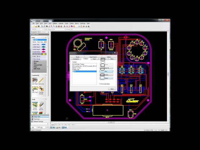
This video shows how to use a mouse in CAM350. The GUI is also discussed as well as how to customize it. Custom toolbars and hot keys are demonstrated
Career Center | Stouffville, Ontario Canada | Engineering,Maintenance,Production,Quality Control,Technical Support
A versatile Facility, Manufacturing and Program Manager with over 18 years of progressive experience in the Electronic Manufacturing Service complimenting the needs of OEM/ECMs in the Automotive, Consumer and Commercial electronics and Datacom and Te
Career Center | Stouffville, Ontario Canada | Engineering,Maintenance,Management,Production,Purchasing,Technical Support
Innovation/Creativity Cost Saving Strategies Employee Motivation Customer Service Focus Program, Repair and Maintenance New Product Development Continuous Improvement Training & Development Process Planning & Labour O
HASL - WHAT A HASSLE, or HASL'd AGAIN. If you don't see the images, please visit online version at #Application.SmtNet.baseURL#/express/ Featured Article HASL - WHAT A HASSLE, or HASL'd AGAIN. Proof Of Design MoonMan This article updates
of accelerated stresses to expose product flaws early in
ASYMTEK Products | Nordson Electronics Solutions | https://www.nordson.com/en/divisions/sonoscan/about/events/events-2021
. Come and see how AMI can help detect flaws non-destructively Non-destructively inspect sensor products, components and assemblies, from wafer, to bonding processes, to final packaging
Imagineering, Inc. | https://www.pcbnet.com/blog/prototyping-circuit-boards-everything-you-need-to-know-before-you-start/
essential phase in any manufacturing process. Having a prototype PCB board will allow you to spot design flaws and address them at this stage


