Industry Directory | Consultant / Service Provider / Manufacturer
Tropical Stencil is dedicated to providing the highest quality Laser Cut Stencils; with our rapid response, you will have your Stencil delivered on-time.
Industry Directory | Consultant / Service Provider / Distributor / Manufacturer / Other
Ludee Circuits offer RoHS PCB.We could offer leadfree HASL,Entek, flash gold, immersion gold, immersion silver, immersion tin finishing based on standard FR-4, CEM-3 materials, Teflon, Rogers RO4000 series, as well as high Tg S1170 materials.
Ridgid, bare board manufacturing of military, high reliability, quick-turn, prototype, single, double-sided, and multilayer boards, blind and buried vias, carbon ink, immersion silver, immersion tin, reflow, hasl, nickel and gold, all colors of legen
Bicheng provides RD, high-tech, IT research companies and organizations, large or small with high quality bare PCB's PCB Products & Services * FR-4, High TG170, High CTI 600V * MCPCB, 1W/mk- 3W/mk * High speed
Electronics Forum | Thu Sep 16 15:01:13 EDT 2004 | russ
You may want to either open up the bottom of the vias so they will not "volcano". Or you will want to seal both sides. It never works having one side of the vias masked and the other open with HASL. Russ
Electronics Forum | Tue Sep 14 14:52:22 EDT 2004 | Carol
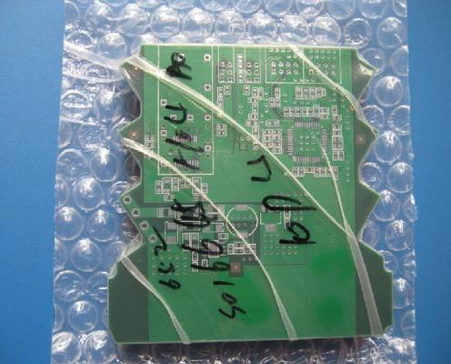
During processing, the solder in the vias reflows and forms solder balls. PCBs have solder in random PBGA vias from the board manufacturer.The manufacturer says this is a result of the HASL process and is unavoidable. We use HASL finish, multilayer,
Industry News | 2008-02-04 11:15:15.0
The European Institute of Printed Circuits (EIPC) extends an invitation to companies and individuals active in the Packaging and Interconnection Industry to submit abstracts for presentation at their Summer Conference which is to be held onMay 29 & 30 2008 in Dresden, Germany.
Technical Library | 2023-03-16 18:51:43.0
Conductive anodic filament (CAF) formation was first reported in 1976.1 This electrochemical failure mode of electronic substrates involves the growth of a copper containing filament subsurface along the epoxy-glass interface, from anode to cathode. Despite the projected lifetime reduction due to CAF, field failures were not identified in the 1980s. Recently, however, field failures of critical equipment have been reported.2 A thorough understanding of the nature of CAF is needed in order to prevent this catastrophic failure from affecting electronic assemblies in the future. Such an understanding requires a comprehensive evaluation of the factors that enhance CAF formation. These factors can be grouped into two types: (1) internal variables and (2) external influences. Internal variables include the composition of the circuit board material, and the conductor metallization and configuration (i.e. via to via, via to surface conductor or surface conductors to surface conductors). External influences can be due to (1) production and (2) storage and use. During production, the flux or hot air solder leveling (HASL) fluid choice, number and severity of temperature cycles, and the method of cleaning may influence CAF resistance. During storage and use, the principal concern is moisture uptake resulting from the ambient humidity. This paper will report on the relationship between these various factors and the formation of CAF. Specifically, we will explore the influences of printed wiring board (PWB) substrate choice as well as the influence of the soldering flux and HASL fluid choices. Due to the ever-increasing circuit density of electronic assemblies, CAF field failures are expected to increase unless careful attention is focused on material and processing choices.
HASL - WHAT A HASSLE, or HASL'd AGAIN. If you don't see the images, please visit online version at #Application.SmtNet.baseURL#/express/ Featured Article HASL - WHAT A HASSLE, or HASL'd AGAIN. Proof Of Design MoonMan This article updates
| https://www.eptac.com/wp-content/uploads/2021/11/webinar_eptac_12_17_08.pdf
Surface Mount Technology Association (SMTA) | https://www.smta.org/knowledge/journal.cfm
., and Gregory Parks Abstract 30-1 3D Wafer Level Packaging by Using Cu-Through Silicon Vias for Thin MEMS Accelerometer Packages L


