Electronics Forum | Sat May 18 15:19:55 EDT 2013 | isd_jwendell
OK, I've now read all of the documents you referenced. The problem still remains regarding the thermal vias and how to minimize scavenging. All the docs acknowledge top and bottom tenting, and it's problems. TI says don't do it. Plugging is usually n
Electronics Forum | Wed Aug 24 21:57:45 EDT 2005 | adeline_ko
The blistering is around the plugging via. I can forward you the pic. For the plugging process, I'm not too sure how they plug. What is the correct practise for the plugging via. Now, what they did is. They will do a tenting process for both side.
Industry News | 2019-11-05 22:07:01.0
Tenting a via refers to covering via with soldermask to enclose or skin over the opening. A via is a hole drilled into the PCB that allows multiple layers on the PCB to be connected to each other. A non tented via is just a via that is not covered with the soldermask layer. Leaving these vias exposed or covered has pros and cons depending on the your design and manufacturing requirements.
Industry News | 2019-11-05 22:08:21.0
Via in pad is the design practice of placing a via in the copper landing pad of a component. Compared to standard PCB via routing, via in pad allows a design to use smaller component pitch sizes and further reduce the PCBs overall size. With component manufactures pushing smaller parts every year and the demand from consumers for smaller devices, the usage of via in pad practices by hardware engineers have become more commonplace. In this article, we will discuss the differences between via in pad and traditional vias, when should you use via in pad, and how to design for it.
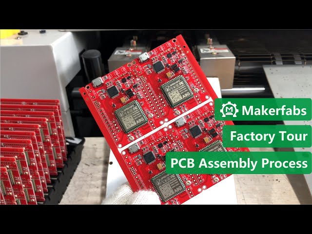
In the world of makers, people enjoy the fun of designing and developing hardware/ software, even final electronic products. They will not concentrate a lot on the cost and manufacturability. But it is quite different from lab to factory, when it com
| https://unisoft-cim.com/test-fixture_download.htm
— Design the Test Fixture The following steps will design the "Bed of Nails" Test Fixture. In this step we will show how to force assign I/O pin numbers for In-Circuit "PURE PIN" ATE testers such as a Teradyne In-Circuit ATE


