Lloyd Doyle designs, manufactures and markets sophisticated automatic optical test (AOT) systems used in the bare board sector of the printed circuit board manufacturing industry.
Industry Directory | Manufacturer
PCB Repairs of all kinds including-Solder on Tab (Solder Removal, Gold Plating), PTH & Delam repairs, etc.
New Equipment | Fabrication Services
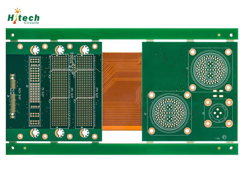
Rigid flex printed circuit boards (PCBs) are manufactured by combining rigid and flexible board technologies. These circuit boards are made up of multiple flexible circuit inner layers. An epoxy pre-preg bonding film is used to attach together these

New Equipment | Rework & Repair Services
On the cutting edge of technology, we offer a full line of high tech services to assist contract manufacturer's and product research and developers. Specializing in quick turn around times to help get your product to market on time. Training Serv
Electronics Forum | Thu Jul 06 16:13:28 EDT 2017 | barryg
Hello everyone, I was curious if anyone knows what criteria there is for layer to layer registration. I have looked at ipc-600 and 601 and have not found anything or am missing something. We had a small qty. of pcbs sent to a customer and some inner
Electronics Forum | Tue Mar 10 04:37:44 EDT 2020 | luciano_zhang
I have a files need produce in a urgent time. It's 4 layers PCB with 3 OZ inner and out layer quantity need 10000pcs ,any one know which supplier is aviliable?
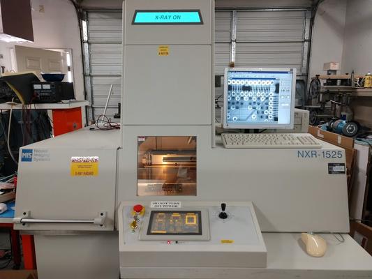
Used SMT Equipment | X-Ray Inspection
This is a used NXR-1525 Xray System can be used to for PCB X-ray inspection of BGA and other SMD Devices. It is a high resolution X-ray system that can show inner layer traces of the Circuit Board. The date of manufacture is September 1999. It
-2 Chip Mounter.jpg)
Used SMT Equipment | Pick and Place/Feeders
Model: YSM20R TypeSV Target board size Monorail model: L810 × W490 ~ L50 × W50 Double conveyor model: ※**X-axis is a model with double beam specifications When sending one board: L810 × W490 ~ L50 × W50 When two boards ar
Industry News | 2003-02-27 08:22:44.0
Circatex is to open its first satellite office in mainland Europe in France.
Industry News | 2010-12-17 01:47:04.0
IPC has released the A revision of IPC-2222, Sectional Design Standard for Rigid Organic Printed Boards. Helping developers avoid common missteps that reduce board manufacturability, IPC-2222 has been expanded to include more information on board materials, such as relative costs, tolerances of board thickness, unsupported holes, and hole aspect ratios.
Parts & Supplies | Pick and Place/Feeders
SM421 X-Axis Driver J31531049A Other Samsung parts in stock: J3212040A PHOTO SENSOR[BGS-2S15N] J71551149A EXTEND_SPRING J7066186A TAPE GUARD SHAFT[SM1-MF32-020] J91841003A SM431_TEACHING_BOX_ASSY J91841003A J9061046D HEAD VACUUM/BLOW ASSY[HD05-
Parts & Supplies | Pick and Place/Feeders
SM421 Track Driver J3153055A Other Samsung parts in stock: J3212040A PHOTO SENSOR[BGS-2S15N] J71551149A EXTEND_SPRING J7066186A TAPE GUARD SHAFT[SM1-MF32-020] J91841003A SM431_TEACHING_BOX_ASSY J91841003A J9061046D HEAD VACUUM/BLOW ASSY[HD05-1]
Technical Library | 2024-09-02 18:48:58.0
The conversion to higher temperature "Lead Free" assembly reflow conditions has created an increased awareness that entrapped or absorbed moisture is a frequent root cause of thermally induced delamination at assembly reflow. There are two connected failure modes from entrapped moisture; incomplete resin cross-linking resulting in premature resin decomposition and also severe Z axis expansion from "explosive vaporization of the entrapped moisture at elevated temperatures at assembly reflow". Ultimately, both result in delamination failure. Other papers have shown the negative effects of entrapped moisture before lamination including delamination, red color, reduced thermal reliability and increased high speed signal loss. In this paper, various materials were tested for moisture sensitivity during lamination. Tests were performed at varying lamination conditions including a pre-vacuum step and "kiss" step. Pressure and cure temperature parameters were evaluated for minimizing or eliminating the effect of trapped moisture. Also included are the results of inner layer moisture removal baking conditions and their effect on peel strength and thermal reliability.
Technical Library | 2011-06-16 18:59:43.0
Based on tests carried out with commercially available chemistry, this paper discusses the advantages available through the use of NEAP processes for inner layer bonding and soldermask pretreatment. The process is characterized with a view to high volume
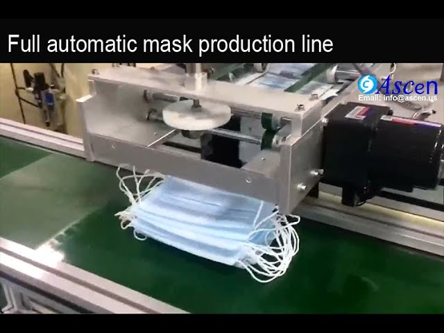
Link: https://www.ascen.ltd/Products/mask_making_machine/ automation medical face mask machine with inner loop welding is automatic from material feeding to mask collection 1.high automation with PLC, photoelectric detection for the raw material feed
Link: https://www.ascen.ltd/Products/mask_making_machine/ automation medical face mask machine with inner loop welding is automatic from material feeding to mask collection 1.high automation with PLC, photoelectric detection for the raw material feed
Events Calendar | Tue Jan 23 00:00:00 EST 2018 - Tue Jan 23 00:00:00 EST 2018 | New Milford, Connecticut USA
FREE Webinar: Eliminate Circuit Board Problems and Failure Modes
Imagineering, Inc. | https://www.pcbnet.com/capabilities/assembly/technology-roadmap/
• Inner Layer - 10 oz • Inner Layer - 16 oz Buried/Blind Via 10+N+10 (HDI) Plasma Desmear Yes Outline Tolerance +/-.004 Surface Finish • HASL • ENIG • Immersion Silver • OSP (ENTEK) • Carbon • Immersion Tin • Electrolyic Gold • ENEPIG • ENIPIG Impeadance Control
PCB Libraries, Inc. | https://www.pcblibraries.com/Forum/ipc7351-padstack-naming-convention_topic36_page3.html
. Inner Layer Land is the same shape as the outer layer land The inner layer land shapes are Circular These 2 statements are conflicting with each other, how can the inner layer land shape be the same
.gif)


winsouce.jpg)