Industry Directory | Other / Manufacturer
Gen Pack Assembly is a contract electronics manufacturer providing PCB assembly, testing, and box-build integration for your mid volume & high mix productions. A trusted partner for over 25 years, Gen Pack is proudly ISO:9001
Industry Directory | Manufacturer
Accu-sembly, Inc. is a subcontract electronic assembly house providing assembly services to many different manufacturers. In the past 25 years, we have worked with hundreds of customers from one man operations to industry-leading corporations.
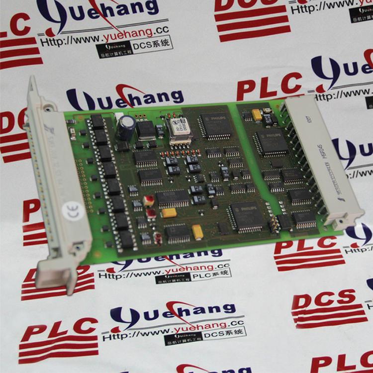
New Equipment | Industrial Automation
Sales Manager: Sandy Lin Email: unity@mvme.cn Skype: onlywnn_1 Mobile(Whatsapp): (+86)-18020776786 XIAMEN YUEHANG COMPUTER ENGINEERING CO.LTD. is a company that professionally engaged in large system DCS spare parts supply. We supply DCS, PLC,
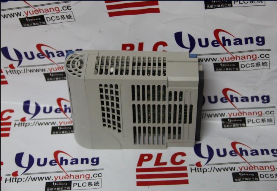
New Equipment | Industrial Automation
Sales Manager: Sandy Lin Email: unity@mvme.cn Skype: onlywnn_1 Mobile(Whatsapp): (+86)-18020776786 XIAMEN YUEHANG COMPUTER ENGINEERING CO.LTD. is a company that professionally engaged in large system DCS spare parts supply. We supply DCS, PLC,
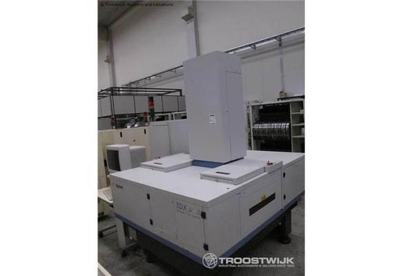
Used SMT Equipment | Visual Inspection
AGILENT, X Ray inspection machine, In line, type 5300-5DX-SERIES 3, SN: US40690565, double top opening, laser class 1, laser subsystem class 3B, equipped with double PC inside, monitor control AGILENT, included small table with standard monitor and k
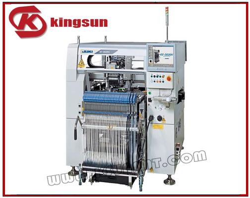
Used SMT Equipment | Pick and Place/Feeders
Product number: KE - 3020VA/ VRA Detailed product introduction Constantly improve the KE series products. So as to realize the high speed highquality electric production line of flexible structure. Chip components 20900 CPH chip (laser identific
Industry News | 2024-06-03 09:36:20.0
IPC releases EMS industry results for April 2024
Industry News | 2023-08-14 12:13:25.0
Count On Tools, Inc. (COT) is pleased to announce its latest advancement in precision component handling – a tailored solution for efficiently handling BrightKing Gas Discharge Tubes and Melf components. This breakthrough solution, part number 2018-3912, is facilitated by the integration of the Custom Yamaha YS12/24 type 318a/307a base and ANE tool stand, enabling customers to achieve precise and reliable pick-and-place operations.
Technical Library | 2021-09-02 08:17:07.0
We are a professional manufacturer of PCB depaneling machines, which is workable for all boards, including flex and regid boards, v-scored boards and routed boards. Laser pcb depaneling is non-contact way without mechanical stress,this solution is good for modern precision PCB depaneling. It has below advantages: 1. No dust The production environment of the circuit board industry is carried out in the dust-free workshop. The traditional pcb depaneling equipment, such as blade moving type machine, will inevitably produce residues and micro powder, which will pollute the 10000 and 1000 class dust-free workshops and affect the conductivity of products. The UV laser PCB cutting machine is a vaporization processing process, which will not produce dust and is conducive to the conductivity of the product. 2. High cutting precision The processing gap of high-precision traditional processing equipment can not reach the gap width of less than 100 microns, which will cause certain damage to the lines on the edge or PCBA circuit board containing components. The focus spot of the laser cutting machine is small, and the ultraviolet cold processing mode has little thermal impact on the edge of the circuit board. The cutting position accuracy is less than 50 microns, and the cutting size accuracy is less than 30 microns, which will not affect the edge of the circuit board, and the precision is high. 3. No stress Traditional processing methods generally have V-grooves, which will cause certain damage to the board in the manufacturing process. The UV laser PCB cutting machine can directly cut the bare board without making V-grooves. In addition, the traditional processing methods directly use tools to act on the circuit board, especially the stamping method has a great impact on the circuit board, which is easy to cause board deformation. The laser cutting machine is a non-contact processing mode, which acts on the surface of the material through the high-energy beam, which will not cause the influence of stress and the deformation and damage of the circuit board. 4. For special-shaped cutting, it is easy to automate The UV laser PCB cutting machine can cut for any shape without replacing any props and fixtures, and without steel mesh. The same equipment can meet special-shaped and straight-line cutting, which is easy to realize assembly line automatic production and high flexibility. It is easy to improve production efficiency and save production process and production cycle. In particular, it can quickly and efficiently meet the needs of rapid proofing, directly import the drawing, and then locate the cutting. 5. High compatibility The UV laser PCB cutting machine can process the materials around the circuit board, such as PCB, FPC, covering film, pet, reinforcing board, IC, ultra-thin metal cutting, etc. it has strong practicability, is compatible with the processing of a variety of materials, is easy to operate, can be imported into the drawing, does not need to adjust any mechanical parts, and is easy to operate and maintain. 6. Good cutting edge effect The cutting edge is smooth and neat without burr. It can be processed and formed directly according to the size of the drawing, which is conducive to improving the yield of the product. It can be directly installed into the subsequent process without further processing. For more details about UV laser depaneling, please feel free to contact us. www.pcbdepanelingrouter.com
Technical Library | 2021-07-20 20:02:29.0
During the manufacturing of printed circuit boards (PCBs) for a Flight Project, it was found that a European manufacturer was building its boards to a European standard that had no requirement for copper wrap on the vias. The amount of copper wrap that was measured on coupons from the panel containing the boards of interest was less than the amount specified in IPC-6012 Rev B, Class 3. To help determine the reliability and usability of the boards, three sets of tests and a simulation were run. The test results, along with results of simulation and destructive physical analysis, are presented in this paper. The first experiment involved subjecting coupons from the panels supplied by the European manufacturer to thermal cycling. After 17 000 cycles, the test was stopped with no failures. A second set of accelerated tests involved comparing the thermal fatigue life of test samples made from FR4 and polyimide with varying amounts of copper wrap. Again, the testing did not reveal any failures. The third test involved using interconnect stress test coupons with through-hole vias and blind vias that were subjected to elevated temperatures to accelerate fatigue failures. While there were failures, as expected, the failures were at barrel cracks. In addition to the experiments, this paper also discusses the results of finite-element analysis using simulation software that was used to model plated-through holes under thermal stress using a steady-state analysis, also showing the main failure mode was barrel cracking. The tests show that although copper wrap was sought as a better alternative to butt joints between barrel plating and copper foil layers, manufacturability remains challenging and attempts to meet the requirements often result in features that reduce the reliability of the boards. Experimental and simulation work discussed in this paper indicate that the standard requirements for copper wrap are not contributing to the overall board reliability, although it should be added that a design with a butt joint is going to be a higher risk than a reduced copper wrap design. The study further shows that procurement requirements for wrap plating thickness from Class 3 to Class 2 would pose little risk to reliability (minimum 5 μm/0.197 mil for all via types).Experimental results corroborated by modeling indicate that the stress maxima are internal to the barrels rather than at the wrap location. In fact, the existence of Cu wrap was determined to have no appreciable effect on reliability.

This video outlines the IPC-A-620 certification and training program and wires and terminals. It describes the program, the materials and provides a good general overview of the class outline. Visit Our Site For More Information About IPC IPC WHMA-A

This video describes the J-STD-001 solder certification program. It is an overview of the program, the certification requirements and the types of credentials. For More Information On IPC J-STD-001 Training Visit Our Website: IPC J-STD-001 CIT Cert
Training Courses | | | IPC J-STD-001 Space Specialist (CIS)
The J-STD-001 Space Addendum is an additional optional module for the Certified IPC J-STD-001 CIS (Specialist) program for organizations that are required to meet these additional requirements.
Training Courses | | | IPC J-STD-001 Space Trainer (CIT)
The IPC J-STD-001 Space Addendum (CIT) certification courses allow individuals to conduct Certified IPC J-STD-001 Space Addendum Specialist (CIS) training.
Career Center | Newbury Park, California USA | Engineering,Maintenance,Production,Quality Control
MUST BE: Proficient with Stencil Print Operations. Familiarity with SMT component types and packages. Ability to read and understand procedure document and work instructions. Operate fully automated SMT, Surface Mount Lines including: Screen Pr
Career Center | Nashville, North Carolina USA | Production
MUST BE WILLING TO BECOME FULLY VACCINATED FOR COVID-19, OR QUALIFY FOR A RECOGNIZED EXEMPTION, TO WORK AT ACDI IF GOVERNMENT CONTRACTOR REGULATIONS ARE UPHELD. OUR COMPANY What we do day-in and day-out has a lasting, meaningful impact across man
Career Center | KANPUR, UTTAR PRADESH India | Engineering,Management,Production
1)Responsible for Implementation of Process Control of SMT /Thru hole components assembly consisting of packages like BGA,MICRO BGA,QFP,PLCC and similar packages on the PCB�s/hybrids, wave soldering as well as reflow soldering processes., Testing of
Career Center | Parwanoo, Himachal Pradesh India | 2016-06-29 04:36:44.0
Engineering
| https://www.eptac.com/faqs/soldertips/soldertip/soldertip-39-class-2-vs-class-3-assemblies
: Class 2 vs Class 3 Assemblies Question: Can you give me a basic definition of the differences between Class 2 and Class 3 products and where these differences show up in the IPC documents? Possible Solution
PCB Libraries, Inc. | https://www.pcblibraries.com/Forum/ipc-class_topic2176_post9013.html
. IPC Class 2 - Dedicated Service Electronic Products – Includes products where continued performance and extended life is required, and for which uninterrupted service is desired but not critical