Industry Directory | Manufacturer
Juivtmall is a PCB manufacture, produce normal PCB, FPC and HDI As for 2-layer, default property, the lead time will be 1 day. Ability of produce: Layer: 2-64 layers Min drill: 0.1mm Min trace/spacing: 1.57mil 2+N+2, 3+N+3......
Industry Directory | Consultant / Service Provider
Quick Turn PCBs, 5 Prototype PCBs at $25.00ea. Fast5Protos delivers quality PCBs in 1-2 days. Free tooling, test, & shipping.
New Equipment | Fabrication Services
HDI PCB Manufacturer & Assembly – One-stop services from China -HDI (high-density interconnection board) is a compact circuit board designed for small capacity users. Compared with ordinary PCB, the most significant feature of HDI is that the wiri
Up to 20 layers, 4 mil traces / spaces, 6 mil drilled holes and Book-bind capability. MIL-P-50884 approved for adhesiveless materials. Deliveries down to 3 days are available.
Electronics Forum | Thu Apr 29 09:37:12 EDT 1999 | Dave F
| Can anyone in this world produce such small PCB/PWB trace widths? Lots of theory so far, but have not found anyone yet who can do it in practice. | Daniel: 2 mil lines with 3 mil spaces are pretty technical. Good luck. Dave F
Electronics Forum | Thu Apr 29 10:11:41 EDT 1999 | Cunli
| Can anyone in this world produce such small PCB/PWB trace widths? Lots of theory so far, but have not found anyone yet who can do it in practice. | Dan, I have seen boards with 3 mil pitch (that is 1.5 mil trace and 1.5 mil spacing) in quantity
Used SMT Equipment | In-Circuit Testers
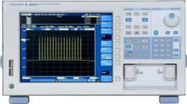
Yokogawa AQ6370 OPTICAL SPECTRUM ANALYZER. The AQ6370 uses a double-pass monochromator structure to achieve high wavelength resolution (0.02 nm) and wide close-in dynamic range (70 dB). Thus, closely allocated signals and noise can be separately

Used SMT Equipment | In-Circuit Testers
Yokogawa AQ6370 OPTICAL SPECTRUM ANALYZER. The AQ6370 uses a double-pass monochromator structure to achieve high wavelength resolution (0.02 nm) and wide close-in dynamic range (70 dB). Thus, closely allocated signals and noise can be separately
Industry News | 2003-03-11 08:45:00.0
CAMtastic DXP is the latest version of Altium's complete CAM verification and editing system that bridges the gap between PCB design and manufacturing and facilitates communication between board designers, fabrication engineers, and their clients.
Industry News | 2018-10-18 11:15:12.0
PCB Design and Layout Guidelines
Parts & Supplies | Circuit Board Assembly Products
Specifications 1.One-stop OEM pcb assembly service. 2.ROHS, SGS, UL certificated 3.Reasonable price 4.High Quality 5.Fast Delivery PCB Assembly&PCBA Service 1. Experienced components sourcing team specially for scarce parts 2.1 to 12 layers m
Parts & Supplies | Circuit Board Assembly Products
Specifications 1.One-stop OEM pcb assembly service. 2.ROHS, SGS, UL certificated 3.Reasonable price 4.High Quality 5.Fast Delivery PCB Assembly&PCBA Service 1. Experienced components sourcing team specially for scarce parts 2.1 to 12 layers m
Technical Library | 2016-09-08 16:27:49.0
In this investigation a test matrix was completed utilizing 900 electrodes (small circuit board with parallel copper traces on FR-4 with LPI soldermask at 6, 10 and 50 mil spacing): 12 ionic contaminants were applied in five concentrations to three different spaced electrodes with five replicas each (three different bare copper trace spacing / five replications of each with five levels of ionic concentration). The investigation was to assess the electrical response under controlled heat and humidity conditions of the known applied contamination to electrodes, using the IPC SIR (surface insulation resistance) J-STD 001 limits and determine at what level of contamination and spacing the ionic / organic residue has a failing effect on SIR.
Technical Library | 2021-06-21 19:34:02.0
In this era of electronics miniaturization, high yield and low-cost integrated circuit (IC) substrates play a crucial role by providing a reliable method of high density interconnection of chip to board. In order to maximize substrate real-estate, the distance between Cu traces also known as line and space (L/S) should be minimized. Typical PCB technology consists of L/S larger than 40 µ whereas more advanced wafer level technology currently sits at or around 2 µm L/S. In the past decade, the chip size has decreased significantly along with the L/S on the substrate. The decreasing chip scales and smaller L/S distances has created unique challenges for both printed circuit board (PCB) industry and the semiconductor industry. Fan-out panel-level packaging (FOPLP) is a new manufacturing technology that seeks to bring the PCB world and IC/semiconductor world even closer. While FOPLP is still an emerging technology, the amount of high-volume production in this market space provide a financial incentive to develop innovative solutions in order to enable its ramp up. The most important performance aspect of the fine line plating in this market space is plating uniformity or planarity. Plating uniformity, trace/via top planarity, which measures how flat the top of the traces and vias are a few major features. This is especially important in multilayer processing, as nonuniformity on a lower layer can be transferred to successive layers, disrupting the device design with catastrophic consequences such as short circuits. Additionally, a non-planar surface could also result in signal transmission loss by distortion of the connecting points, like vias and traces. Therefore, plating solutions that provide a uniform, planar profile without any special post treatment are quite desirable.
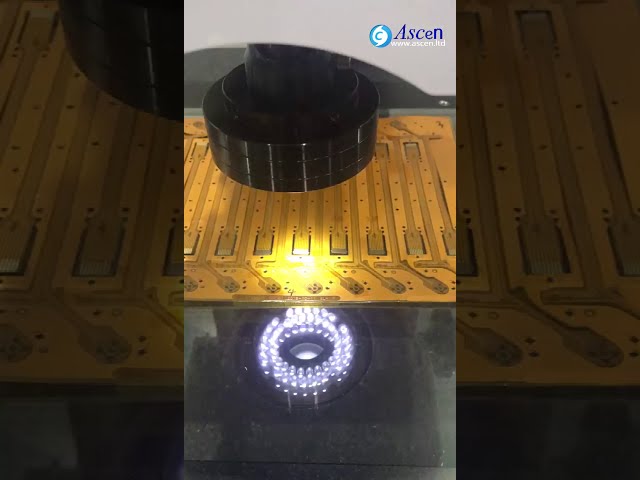
https://www.ascen.ltd/Products/PCB_board_assembly_system/vision_measurin/507.html Vision Measuring Machine and image measuring instrument can be used for dimensional accuracy measurement of various molds, aircraft, automobile, mobile phone, computer,
https://www.ascen.ltd/Products/PCB_board_assembly_system/vision_measurin/507.html Vision Measuring Machine and image measuring instrument can be used for dimensional accuracy measurement of various molds, aircraft, automobile, mobile phone, computer,
Training Courses | | | IPC-600 Specialist (CIS)
The Certified IPC-600 Specialist (CIS) training targets quality assurance and acceptance of bare printed circuit boards.
Training Courses | | | IPC-7711/7721 Specialist (CIS)
The Certified IPC-7711/7721 Specialist (CIS) training focuses on rework of electronic assemblies and repair and modification of printed boards and electronic assemblies.
Career Center | Erode, Tamilnadu India | Engineering
Professional Summary 3+ years of experience in the PCB CAM engineering Exposure to FRONTLINE GENESIS 2000 Having exposure in UCAM Exposure to Create, Array & Panelize it for manufacturability Experienced in Creating impedance cou
| https://www.eptac.com/etrainings/ipc-designer-certification-online/
“Generic Standard on Printed Board Design” and IPC-2222 “Sectional Design Standard for Rigid Organic Printed Boards”. The program covers guidance and requirements for printed board assembly and design parameters from component mounting, interconnecting structures, conductor characteristics, surface finishes, board
| https://unisoft-cim.com/pcbtest.php
. The Unisoft ProntoTEST-FIXTURE software translates CAD or Gerber and Bill of Materials (BOM) files into real reference designators, X/Y component pins, nets, trace runs, rotation, part numbers, etc


