New Equipment | Assembly Services
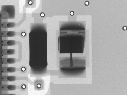
If you are an EMS provider or OEM of electronic/electrical components or sub-assemblies incorporating plastics, metals, ceramics or any combination of these, BEST Inc can offer you knowledgeablePCB x-ray inspection services. BEST experiences in thes
Industry News | 2003-01-31 09:39:08.0
Expected to be Below the Guidance Provided During the Company's Earnings Conference Call on December 18, 2002
Industry News | 2018-02-19 13:55:53.0
IPC — Association Connecting Electronics Industries® Pb-free Electronics Risk Management (PERM) Council has developed the first single document dedicated solely to assisting design engineering in the development of electronics that are completely lead-free (Pb-free) and meet the demanding requirements of aerospace, defense and high performance (ADHP) products and systems.
Technical Library | 2023-01-17 17:27:13.0
Reflow profile has significant impact on solder joint performance because it influences wetting and microstructure of the solder joint. The degree of wetting, the microstructure (in particular the intermetallic layer), and the inherent strength of the solder all factor into the reliability of the solder joint. This paper presents experimental results on the effect of reflow profile on both 63%Sn 37%Pb (SnPb) and 96.5%Sn 3.0%Ag 0.5%Cu (SAC 305) solder joint shear force. Specifically, the effect of the reflow peak temperature and time above solder liquidus temperature are studied. Nine reflow profiles for SAC 305 and nine reflow profiles for SnPb have been developed with three levels of peak temperature (230 o C, 240 o C, and 250 o C for SAC 305; and 195 o C, 205 o C, and 215 o C for SnPb) and three levels of time above solder liquidus temperature (30 sec., 60 sec., and 90 sec.). The shear force data of four different sizes of chip resistors (1206, 0805, 0603, and 0402) are compared across the different profiles. The shear force of the resistors is measured at time 0 (right after assembly). The fracture surfaces have been studied using a scanning electron microscopy (SEM) with energy dispersive spectroscopy (EDS)
Technical Library | 2007-08-16 13:34:31.0
While experienced inspectors may be able to determine the aesthetic differences between a lead-free PCB assembly and a tin-lead version, one cannot rely on the "experienced eye". "Less wetting out to the pad edges" (Figure A) and "graininess and lack of shininess of the solder joint" (Figure B) are typical comments about some lead-free solder joints. However, in cases where a Nitrogen atmosphere was present during the reflow of the solder joint (Figure C), there will be little visual differences between the lead free alloys and their tin-lead counterparts.

http://www.gpd-global.com No drip no drool across a wide range of fluid viscosities (low-to-mid and low-to-high). No manual adjustment to compensate for pump variability. Truly Volumetric PCD Pumps for total control of dispensing fluids. Ability to
BGA integrated circuits and chip scale packages, CSPs where the solder connections are not visible. This has arisen as a result of the need for greater numbers of interconnections to integrated circuit packages and as a general result of increasing c
Head-in-Pillow BGA Defects Head-in-Pillow BGA Defects. Head-in-pillow (HiP), also known as ball-and-socket, is a solder joint defect where the solder paste deposit wets the pad, but does not fully wet the ball. This results in a solder joint
| http://etasmt.com/cc?ID=te_news_industry,24564&url=_print
. According to the IPC standard, non-wetting is defined as the inability of molten solder to form a metallic bond with the base metal. This results in the PCB pads or the
| https://www.eptac.com/wp-content/uploads/2021/11/webinar_eptac_08_19_09.pdf
7.6.4 Dim G states that “wetting is evident” Is it implied or specified the amount of the joint that must show wetting? 11 #4 Wetting is Evident


winsouce.jpg)