
Industry Directory | Consultant / Service Provider / Media / Publisher / Online Resource / Other
PCB Libraries' "Footprint Expert" suite uses CAD LEAP(tm) Technology to greatly simplify footprint and 3D STEP model creation; it is used by tens of thousands of PCB designers and engineers all over the world.
Industry Directory | Consultant / Service Provider
PCB Matrix is dedicated to creating and delivering software tools that simplify and automate electronic product development.
New Equipment | Education/Training
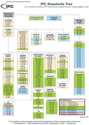
IPC standards, the results of industry consensus and collaboration, are respected throughout the whole world. Using IPC standards allows manufacturers, customers and suppliers to speak the same language. IPC standards are used by the electronics

The PCB Footprint Expert is a powerful CAD library development tool powered by our own proprietary CAD LEAP Technology (Libraries Enhanced with Automated Preferences). It is packed with very powerful advanced library management features that cuts foo
Electronics Forum | Fri Mar 29 10:51:20 EST 2002 | lsmith
The IPC-EM-782 reads as follows: the adjustment factor is usually intended to increase the Z dimension slightly, but brings the Z maximum up to an even equivalent. Example if Zmax is 2.100mm then you would enter an adjustment factor of .100mm. The ad
Electronics Forum | Thu Mar 21 15:36:19 EST 2002 | slthomas
We're having trouble with a TO-252 DPAK from Fairchild (MC7805CDT) and our existing land pattern. The land pattern calculator on the IPC site doesn't have anything available that matches it (there are no TO-252's available on the pull downs), and I'

Used SMT Equipment | In-Circuit Testers
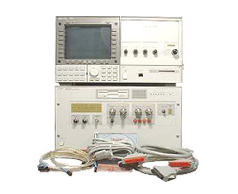
Agilent 71612B-UHF Digital Transmission Tester 12Gb/s The 71612B error performance analyzer addresses applications for high speed digital testing up to 12 Gb/s, including R&D and manufacturing test of lightwave components and sub-assemblies, ad
Used SMT Equipment | In-Circuit Testers
Agilent-Keysight 71612B-UHF Digital Transmission Tester 12Gb/s The 71612B error performance analyzer addresses applications for high speed digital testing up to 12 Gb/s, including R&D and manufacturing test of lightwave components and sub-assem
Industry News | 2013-05-20 16:19:35.0
IPC – Association Connecting Electronics Industries® has teamed up with PCB Libraries, Inc.
Industry News | 2010-07-22 22:37:02.0
IPC — Association Connecting Electronics Industries® has released the B revision of IPC-7351, Generic Requirements for Surface Mount Design and Land Pattern Standard. The leading industry standard for surface mount land pattern design and layout, IPC-7351B provides designers and printed board fabricators with updated guidance on requirements of land pattern geometries used for the surface attachment of electronic components, as well as surface mount design recommendations for achieving the best possible solder joints.

The PCB Footprint Expert is a powerful CAD library development tool powered by our own proprietary CAD LEAP Technology (Libraries Enhanced with Automated Preferences). It is packed with very powerful advanced library management features that cuts foo
UV Laser PCB Depaneling System, Dual Table for High Volume Laser Depaneling Purpose: The processing and application objects are PCB, FPC soft and hard plate and related material cutting, cover opening and other operations. Efficient integration
Training Courses | | | Other Courses
Other courses related to electronics manufacturing and assembly
Training Courses | ON DEMAND | | IPC-600 Trainer (CIT)
The Certified IPC-600 Trainer (CIT) courses recognize individuals as qualified trainers in the area of quality assurance of bare printed circuit boards and prepare them to deliver Certified IPC-600 (CIS) training.
Events Calendar | Mon Jun 10 00:00:00 EDT 2024 - Mon Jun 10 00:00:00 EDT 2024 | Carlsbad, California USA
San Diego Chapter In-Person Event: IPC J-STD-001 Compliant Solder Pattern Calculations for DFA
Events Calendar | Thu Oct 03 00:00:00 EDT 2019 - Thu Oct 03 00:00:00 EDT 2019 | ,
IPC Tech Ed Webinar Series: Ball Grid Array (BGA) and Bottom Termination Component (BTC) Design and Assembly Challenges: Reflow Profiling to Achieve Low Defect Rates and Successful Assembly! – Part 2
Career Center | Auckland, New Zealand | Engineering
NAVMAN PCBA NPI Engineer Reporting To: PCBA NPI Technical Leader Primary Objective: Transition of PCBs from R&D design to a manufacturable state conforming to all facets of PCBA production Secondary: Develop DFM & best practice guidelines Res
Career Center | Sherman, Texas USA | Engineering,Production,Research and Development,Technical Support
SMT Packaging Engineer: Location: Texas - Sherman , TX Group: HVAL Degree Requirements: BS ME/ChemE/Materials The person in this position will have the ability to make very significant financial contributions to TI because this is a very critic
Career Center | Daviddav, India | Engineering,Maintenance,Production,Quality Control,Research and Development
Created and defined component landing patterns for high density layouts beyond the specifications of IPC standards and in compliance with RoHs. • Designing SMT stencils (Solder paste & Glue(Epoxy) stencils).
ASYMTEK Products | Nordson Electronics Solutions | https://www.nordson.com/en/divisions/adhesive-dispensing-systems/products/applicators/miniblue-ii-long-life-hot-melt-dispensing-guns
Unilever Saves Time and Money with MiniBlue II Mars Pet Food Case Study "Why Choose Nordson?" Brochure Technical Tools Adhesive Bead Savings Calculator
| https://unisoft-cim.com/crosschecking-pcb-component-footprint-and-bom-footprint.html
(correct solder pad size and land pattern) for the same component listed in the Bill of Materials (BOM). The mismatch of component footprint spacing is usually an error created when components on the PCB assembly ( PCBA


