New Equipment | Rework & Repair Services
BGA Rework Services Offered BGA Remove and Placement Level Three Pad Repair Wire Add Trace Repair BGA Re-Balling BGA Inspection We Rework PBGA (Plastic Ball Grid Array) TBGA (Tape Ball Grid Array) uBGA (Micro BGA) CCGA (Ceramic Colum
New Equipment | Rework & Repair Services
Reliable LGA Rework Services to Rescue Your Project BEST is your source for LGA rework services. We can optimize our processes to make sure voiding is minimized and the interconnection to all of the IO meets the IPC classification for the assembly.
Electronics Forum | Sat May 30 01:31:49 EDT 2009 | mika
make 4 square rounded corner apertures on the ground pad and the total reduction of 20 % (80 % solder paste). Then you still be able to solder the terminals around. Don't worry to much of the void's. Just following my tips and you will be fine. The
Electronics Forum | Wed Jun 03 13:56:09 EDT 2009 | mika
less total area of voids, which mean a much more strength in the joint and much easier to solder such a cooling pad grounded via vias, with this approach! The same goes for big cooling pads of let say Power transistors without any via etc. Always re
Industry News | 2018-08-16 19:58:50.0
The SMTA Capital Chapter is holding its upcoming Capital Expo and Tech Forum at Johns Hopkins University / Applied Physics Lab, Kossiakoff Center, 11100 Johns Hopkins Road, Laurel, MD 20723, on Thursday, August 23rd.
Industry News | 2018-12-08 03:29:29.0
SMT Dictionary – Surface Mount Technology Acronym and Abbreviation
Technical Library | 2018-09-26 20:33:26.0
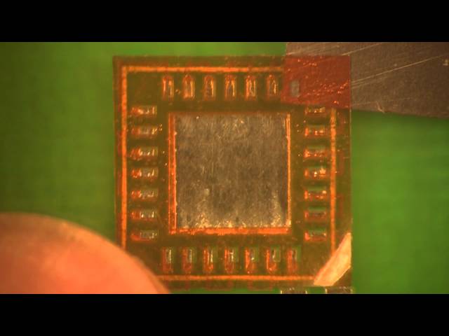
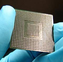
Bottom terminated components, or BTCs, have been rapidly incorporated into PCB designs because of their low cost, small footprint and overall reliability. The combination of leadless terminations with underside ground/thermal pads have presented a multitude of challenges to PCB assemblers, including tilting, poor solder fillet formation, difficult inspection and – most notably – center pad voiding. Voids in large SMT solder joints can be difficult to predict and control due to the variety of input variables that can influence their formation. Solder paste chemistries, PCB final finishes, and reflow profiles and atmospheres have all been scrutinized, and their effects well documented. Additionally, many of the published center pad voiding studies have focused on optimizing center pad footprint and stencil aperture designs. This study focuses on I/O pad stencil modifications rather than center pad modifications. It shows a no-cost, easily implemented I/O design guideline that can be deployed to consistently and repeatedly reduce void formation on BTC-style packages.
Technical Library | 2015-07-14 13:19:10.0
Bottom terminated components (BTC) are leadless components where terminations are protectively plated on the underside of the package. They are all slightly different and have different names, such as QFN (quad flat no lead), DFN (dual flat no lead), LGA (land grid array) and MLF (micro lead-frame. BTC assembly has increased rapidly in recent years. This type of package is attractive due to its low cost and good performance like improved signal speeds and enhanced thermal performance. However, bottom terminated components do not have any leads to absorb the stress and strain on the solder joints. It relies on the correct amount of solder deposited during the assembly process for having a good solder joint quality and reliable reliability. Voiding is typically seen on the BTC solder joint, especially on the thermal pad of the component. Voiding creates a major concern on BTC component’s solder joint reliability. There is no current industry standard on the voiding criteria for bottom terminated component. The impact of voiding on solder joint reliability and the impact of voiding on the heat transfer characteristics at BTC component are not well understood. This paper will present some data to address these concerns.
Training Courses | | | PCB Rework and Hand Soldering Courses
The PCB rework and hand soldering courses courses cover techniques of rework and repair of PCBs, BGAs and other electronics assemblies, and teach fundamentals of soldering of electronics assemblies.
Training Courses | | | PCB Rework and Hand Soldering Courses
The PCB rework and hand soldering courses courses cover techniques of rework and repair of PCBs, BGAs and other electronics assemblies, and teach fundamentals of soldering of electronics assemblies.
SMTnet Express, September 27, 2018, Subscribers: 31,354, Companies: 11,055, Users: 25,237 Assessing the Effectiveness of I/O Stencil Aperture Modifications on BTC Void Reduction Carlos Tafoya, Gustavo Ramirez, Timothy O'Neill; AIM Solder Bottom
| https://pcbasupplies.com/s3x58-m650-7-600gm/
residue over the solder joint, which helps the testing probe to get the accurate readings to improve the first pass rate. Resistance between Probe and PCB Superior wetting ability prevents voiding For smaller components such as QFNs, micro BGA and LGA, bigger voids could occupy majority of the pad area thus creating a
Surface Mount Technology Association (SMTA) | https://www.smta.org/knowledge/webinars.cfm
Solder Joint Voids - All You Should Know Jennie S. Hwang, Ph.D. $200.00 2017 Advances in Stencil Technology for Achieving Successful Printing Results Chrys Shea Free! 2017