
Industry Directory | Consultant / Service Provider / Equipment Dealer / Broker / Auctions / Manufacturer / Training Provider
SCANSMT is local stocking dealer who major in SAMSUNG,PANASONIC,YAMAHA,JUKI,FUJI mounter and MIRTEC,KOHYOUNG,PARMI,PEMTRON,CYBEROPTICS AOI&SPI,MPM,SJ,ESE Printers.HELLER,TSM Reflows are always have invertonries.welcome to visit us
Industry Directory | Manufacturer
Line Scan Camera india is New Delhi, India based company, We are registered in India under Indian companies’ act 1955. We are Multi-Million USD turnover company & unit of "B.B. Group of Companies".
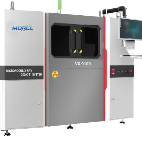
MICROFOCUS X-RAY 3D/CT SYSTEM VX-9100 The VX-9100 3D X-Ray Inspection Machine is a state-of-the-art industrial microfocus CT system designed for precise quality inspection and non-destructive analysis of electronic components. Its advanced cap
.jpg)
Automatic SMT Splicing Machine BMM08G/G_Plus Functional advantages ▶Simple operation: 5 minutes to learn to operate, everyone can operate, reducing dependence on personnel. ▶Foolproof and error-proof: Automatically scan the code to compare and prev
Electronics Forum | Mon Jul 26 03:32:31 EDT 1999 | Jason
| | | Hello, | | | i'm looking for informations about companies which are using system to verify the loadind of a SMT machine by using barcode (on the slot on the machine & on the reel). | | | I'm in charge of the installation of this kind of system
Electronics Forum | Fri Jul 16 17:49:06 EDT 1999 | JohnW
| | Hello, | | i'm looking for informations about companies which are using system to verify the loadind of a SMT machine by using barcode (on the slot on the machine & on the reel). | | I'm in charge of the installation of this kind of system. | |
Used SMT Equipment | SMD Placement Machines
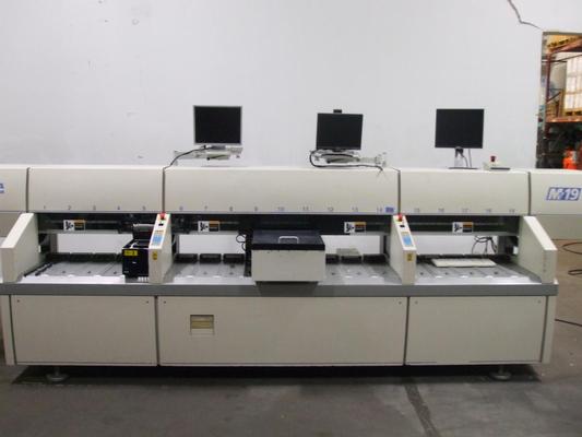
2002 Mydata MY19 SMT Pick & Place Serial: 19148 Features: S/W Version: 2.5.4 2 2 Pole Electrical Test LSC: Line Scan Vision System DVC: Dual Vision System Optical Centering Autoteach
Used SMT Equipment | Pick and Place/Feeders
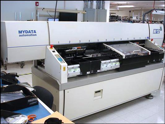
2004 Mydata MY 12 SMT Pick and Place Power: 210 / 121VAC; 3 Phase Machine Dimensions: 132" x 48" x 60" Features: Electrical two-pole test Optical Centering HYDRA; HYDRA High Speed Z High Speed; Autoteach Line Scan Software Version 2.4.6b
Industry News | 2003-03-25 09:15:19.0
The Dragon was demonstrated at the CPCA show in Shanghai last week
Industry News | 2003-04-03 08:51:07.0
Symphony 3070TM Package from JTAG Technologies for Testing and In-System Flash / PLD Programming

Parts & Supplies | Pick and Place/Feeders
KHY-M221A-A0 KGT-M221A-A0 YAMAHA YG12 tank chain gland KHY-M2267-00 YG12 tank chain YS12 towline keel X axis PISCO SP2550 R75 KHY-M2276-S0 YS12 screw X-axis YG12 X-axis screw YG12F YS12F screw guide KHY-M371R-00 RAIL GUIDE 12P YS24 YS100 Feida pl

Parts & Supplies | SPI / Solder Paste Inspection
Quick programming, friendly programming interface Multiple measurement methods True one-button measurement Eight-way motion button, one-click focus Adjustable scanning pitch Solder paste 3D simulation function Powerful SPC function MARK
Technical Library | 2020-03-26 14:55:29.0
This paper introduces line confocal technology that was recently developed to characterize 3D features of various surface and material types at sub-micron resolution. It enables automatic microtopographic 3D imaging of challenging objects that are difficult or impossible to scan with traditional methods, such as machine vision or laser triangulation.Examples of well-suited applications for line confocal technology include glossy, mirror-like, transparent and multi-layered surfaces made of metals (connector pins, conductor traces, solder bumps etc.), polymers (adhesives, enclosures, coatings, etc.), ceramics (components, substrates, etc.) and glass (display panels, etc.). Line confocal sensors operate at high speed and can be used to scan fast-moving surfaces in real-time as well as stationary product samples in the laboratory. The operational principle of the line confocal method and its strengths and limitations are discussed.Three metrology applications for the technology in electronics product manufacturing are examined: 1. 3D imaging of etched PCBs for micro-etched copper surface roughness and cross-sectional profile and width of etched traces/pads. 2. Thickness, width and surface roughness measurement of conductive ink features and substrates in printed electronics applications. 3. 3D imaging of adhesive dots and lines for shape, dimensions and volume in PCB and product assembly applications.
Technical Library | 2017-06-15 00:44:19.0
Ceramics packages are being used in the electronics industry to operate the devices in harsh environments. In this paper we report a study on acoustic imaging technology for nondestructively inspecting underfill layers connecting organic interposers sandwiched between two ceramics substrates.First, we inspected the samples with transmission mode of scanning acoustic tomography (SAT) system, an inspection routine usually employed in assembly lines because of its simpler interpretation criteria: flawed region blocks the acoustic wave and appears darker. In this multilayer sample, this approach does not offer the crucial information at which layer of underfill has flaws. To resolve this issue, we use C-Mode Scanning in reflection mode to image layer by layer utilizing ultrasound frequencies from 15MHz to 120MHz. Although the sample is thick and contains at least 5 internal material interfaces, we are able to identify defective underfill layer interfaces.
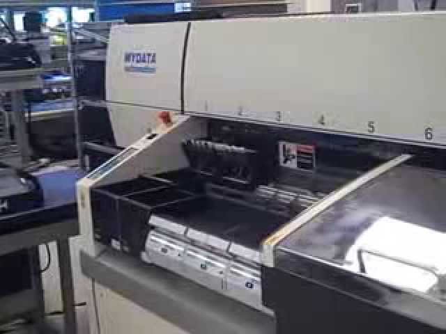
Make: Mydata Make: My100LXe-10 Model: 2013 Software Release: TPSys 2.9x Linux Details: • Midas • HYDRA 3 Speedmount Z8L • LineScan Vision System • DVS Upgrade • T3 Board Handling •
Training Courses | | | PCB Inspection Courses
The PCB inspection courses focus on improving PCB yield and reliability through validation and detection of defects on electronics assemblies.
Training Courses | | | Other Courses
Other courses related to electronics manufacturing and assembly
Career Center | San Diego, California USA | Engineering
Test Engineer in manufacturing environment. Contractor will support Sr Test engineer in new product introductions. Utilize automated In Circuit test equipment to test dual and single sided SMT boards. MUST have current experience with Agilent 3070 l
Career Center | ELLENWOOD, Georgia USA | Production,Quality Control,Research and Development,Technical Support
SMT MACHINE OPERATION, FORKLIFT CERTIFY, SUPERVISION OF MANUFACTURING AND PRODUCTION, QUALITY CONTROL TECH., AUDIO ENGINEER SKILLS,,SET-UP OF MUSICIAL THEMES AND PLAYS.
Career Center | Woodbury, Minnesota USA | Management,Production
Over 20 yrs experience in SMT. Worked with medical, industrial, communications, aerospace and automotive electronics. Have experience working in ITAR controlled companies.
SMTnet Express February 14, 2013, Subscribers: 26181, Members: Companies: 13288, Users: 34310 Boundary Scan Advanced Diagnostic Methods Boundary-scan (1149.1) technology was originally developed to provide a far easier method to perform digital DC
| http://etasmt.com/cc?ID=te_news_news,26365&url=_print
I.C.T is a manufacturer of SMT machines. It mainly provides customers with SMT production lines including SMT Stencil Printers , Pick and place machines , Reflow Oven , AOI Machine , Wave Soldering Machine
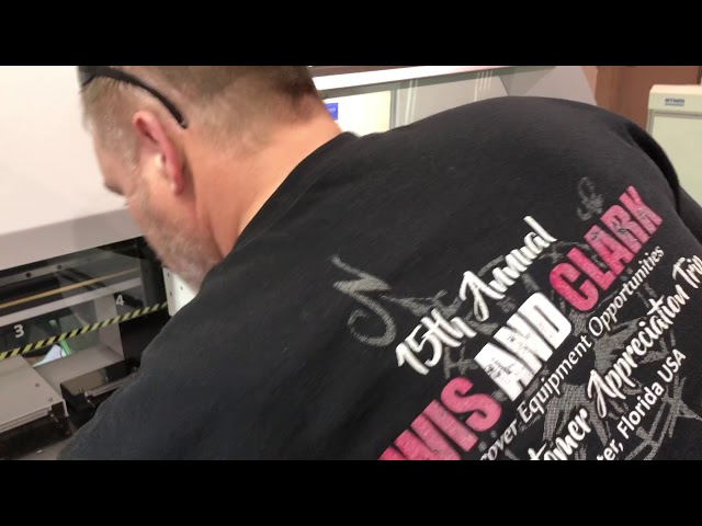
Lewis & Clark | https://www.lewis-clark.com/product/spea-4040-flying-probe/
; 24 lines / sec • Local Area Network System connection with RJ45, driver and Lan interface for 4040 • V/I Generator; Precision Driver, 4Q, ±10V, ±1A • V/I Generator
SCANSMT is local stocking dealer who major in SAMSUNG,PANASONIC,YAMAHA,JUKI,FUJI mounter and MIRTEC,KOHYOUNG,PARMI,PEMTRON,CYBEROPTICS AOI&SPI,MPM,SJ,ESE Printers.HELLER,TSM Reflows are always have invertonries.welcome to visit us
Training Provider / Manufacturer / Equipment Dealer / Broker / Auctions / Consultant / Service Provider
Floor 1,D Building,B area,Dongsheng Techwin Park,Bao'an District
Shenzhen, 30 China
Phone: 008618566662725


