Industry Directory | Manufacturer
Since 1971, Eagle Electronics Inc. has provided our Customers with the highest quality Printed Circuit Boards at fair and competitive prices.
New Equipment | Fabrication Services
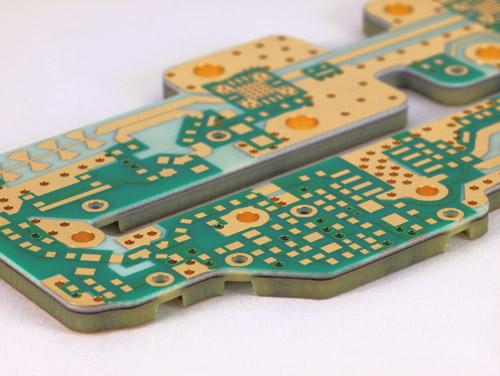
Multilayer PCB's ACI manufactures a wide variety of Multilayer PCB's for various applications spanning numerous industries and technologies. We can build your high layer count PCB's using a wide variety of high speed low loss materials from epoxies
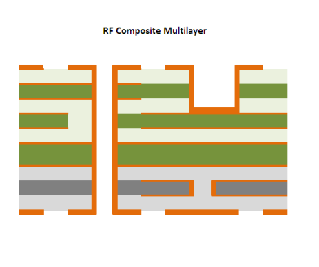
Consisting of multiple laminates and differing dielectric constants, this multilayer (displayed right) is a mixed-dielectric printed circuit board which was manufactured for the Aerospace Industry. Multilayer Mixed Dielectric PCB Specifications:
Electronics Forum | Mon Jul 01 16:15:02 EDT 2002 | Matt Kehoe
We are currently trying to gather information pertaining to applying LPI soldermask thicker than normal. The thick coating is necessary for the SIPAD ssd process however, because of the numerous brands of mask and application methods there is no sing
Electronics Forum | Mon Apr 22 15:05:47 EDT 2002 | tim_easterling
Depending on the volume of boards you are manufacturing, the most cost effective solution would be to epoxy plug the vias prior to LPI soldermask application. The technique is common practice and most suppliers can provide it will little or no cost a
Industry News | 2019-11-05 22:07:01.0
Tenting a via refers to covering via with soldermask to enclose or skin over the opening. A via is a hole drilled into the PCB that allows multiple layers on the PCB to be connected to each other. A non tented via is just a via that is not covered with the soldermask layer. Leaving these vias exposed or covered has pros and cons depending on the your design and manufacturing requirements.
Technical Library | 2016-09-08 16:27:49.0
In this investigation a test matrix was completed utilizing 900 electrodes (small circuit board with parallel copper traces on FR-4 with LPI soldermask at 6, 10 and 50 mil spacing): 12 ionic contaminants were applied in five concentrations to three different spaced electrodes with five replicas each (three different bare copper trace spacing / five replications of each with five levels of ionic concentration). The investigation was to assess the electrical response under controlled heat and humidity conditions of the known applied contamination to electrodes, using the IPC SIR (surface insulation resistance) J-STD 001 limits and determine at what level of contamination and spacing the ionic / organic residue has a failing effect on SIR.


winsouce.jpg)