.jpg)
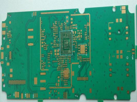
Layer Count: 8L Board Thickness: 1.0mm Panel Dimension:190*86mm/2up Material: S1141 Copper on board surface: 35μm Min Hole Diameter: 0.1mm Min line Width/Space: 8/8mil Surface Finish: ENIG+Selective OSP in BGA area This quick turn PCB is manufacture
New Equipment | Fabrication Services
8 Layers Printed Circuit Boards Manufacturing Multilayer PCB Fabrication Product Name: Multilayer PCB Board Material: FR4 Copper thickness 1 oz all layers Board Thickness: 1.6mm Special requirement Impendence Control Fab by Circuit Boar
Electronics Forum | Tue Nov 11 12:49:13 EST 2003 | Carol
Could you direct me to a Standard or Study that has used this termination with 67/37 tin/lead solder please? I am looking for the recommended reflow temperature requirements and reliability issues for the completed product. We are receiving this type
Electronics Forum | Thu Nov 13 20:48:04 EST 2003 | davef
There a number of studies like this published by component fabricators. Many can be found on the net. For instance: http://www.amd.com/us-en/assets/content_type/DownloadableAssets/Pb-free_Board-level_reliability_study.pdf
Industry News | 2016-08-19 05:00:52.0
If you have a process problem, let NPL Defect of the Month Video help you team
Industry News | 2006-06-23 16:19:47.0
Group Addresses Assembly Process and Reliability Requirements for SnPb and Pb-free Modules
Technical Library | 2023-08-04 15:27:30.0
A designed experiment evaluated the influence of several variables on appearance and strength of Pb-free solder joints. Components, with leads finished with nickel-palladium-gold (NiPdAu), were used from Texas Instruments (TI) and two other integrated circuit suppliers. Pb-free solder paste used was tin-silver-copper (SnAgCu) alloy. Variables were printed wiring board (PWB) pad size/stencil aperture (the pad finish was consistent; electrolysis Ni/immersion Au), reflow atmosphere, reflow temperature, Pd thickness in the NiPdAu finish, and thermal aging. Height of solder wetting to component lead sides was measured for both ceramic plate and PWB soldering. A third response was solder joint strength; a "lead pull" test determined the maximum force needed to pull the component lead from the PWB. This paper presents a statistical analysis of the designed experiment. Reflow atmosphere and pad size/stencil aperture have the greatest contribution to the height of lead side wetting. Reflow temperature, palladium thickness, and preconditioning had very little impact on side-wetting height. For lead pull, variance in the data was relatively small and the factors tested had little impact.
Surface Mount Technology Association (SMTA) | https://www.smta.org/knowledge/journal.cfm
. Schueller, Ph.D., W. Ables, and J. Fitch, Ph.D. Abstract 22-1 INVESTIGATION OF IMC GROWTH IN TIN SURFACE FINISH AND ITS EFFECT ON SOLDERABILITY IN FC-CSP PACKAGING HyunJung Lee, YeonSeop Yu, HyoJung Kim, Hee-Soo Kim Abstract 22-1 COMPREHENSIVE METHODOLOGY TO


